The founder and General Manager of Bolite Optoelectronics, Dr. Bowen Cheng, was invited to present at the recent Touch Taiwan 2021 Conference in April. The title of his talk was “Laser Processing Applications for the Manufacturing of Mini and MicroLED Displays.†Since it was presented in Mandarin only, microled-info.com caught up with Dr. Cheng to learn more about this trending subject and the company he started.
")
Q: Dr. Cheng, can you please tell us a little about your background, prior to starting Bolite?
I was a research engineer at Xerox PARC and helped develop surface micromachined microspring interconnects in a project funded by the U.S. Army Research in collaboration with Oracle. I was also a vital member of the team that successfully demonstrated the world's shortest wavelength diode laser at the time, a 250 nm UV laser for military applications. With these experiences in both semiconductor laser processing and MEMS processing, I decided to start Bolite and build a team to develop state-of-the-art laser solutions for microprocessing applications.
Q: I must admit I’ve not heard of Bolite before. What differentiates you from other laser microprocessing companies?
We are based in Taiwan, and our core values are agility, flexibility, and innovation. What makes our laser solution so uniquely advanced is that our highly talented team has accumulated a lot of know-how over the past 10-plus years. Therefore, we can achieve extremely tight control of the micro-scale thermal behavior of laser-materials interactions, accomplished in both time and spatial domains while integrating lasers with multiple wavelengths. One significant benefit of a laser system with multiple wavelengths is the selective processing of heterogeneous structures with different layer stack-ups. For example, we can drill vias in one layer without thermally damaging an underlying layer of another material.
With the technical capabilities just described, we can also achieve ultra-fine feature sizes and high-level precision positioning. To date, using galvanometer scanning, we have been able to demonstrate laser marking with spots down 0.8 µm diameter and pitch of 1 µm. We can also selectively program at which exact location whether the laser fires or not, as seen in the video below.
Q: OK, now let's get into the main focus of your presentation at Touch Taiwan, namely, what are some of the major laser applications for the manufacturing of mini and microLED displays?
Laser is finding applications in the processing stages of Mass Transfer, Inspection and Repair. First and foremost, there is the Selective Laser Lift-Off (LLO) process: In most microLED flat-panel display manufacturing, microLEDs are fabricated on gallium nitride (GaN) films grown on sapphire wafers. The GaN-based microLED chips are then bonded onto a temporary carrier, and the sapphire substrate is separated from the GaN interlayer via the LLO process. Even though this is a reasonably well-established laser process, by integrating beam-shaping, coaxial imaging, and galvanometer scanning, Bolite offers the added advantage of precise, individual LED selectivity.
As most of us following this field's development are aware, one of the biggest challenges to microLED manufacturing for broad market adoption is how to address the subsequent mass transfer process. Since for a 4K display, even the fastest pick-and-place tool today will take several weeks to transfer the tens of millions of pixels onto the backplane. We are not even considering the yield impact due to the placement accuracy requirement of a few microns. Since the pitch of the microLEDs and the display backplane panel for each RGB pixel will be quite different, Bolite has developed a laser-based pitch re-engineering process based on selective LLO for a sequence of bonding/de-bonding steps. There are several ways to accomplish the pitch-matching, one of which is simply through the controlled expansion of the carrier substrate. Another approach is via chiplets comprised of RGB LEDs and micro-ICs. We have successfully demonstrated selective LLO of microLEDs as small as 20x10 µm from their substrate with high precision (see image below). Scanning speed can be as high as 1 µs per LED.
 Selective Laser Lift-Off (Bolite)
As a final step to this mass transfer path, we have also developed a Laser Assisted Bonding process for various metals and solders (see image below). This process has stringent requirements regarding processing speed, accuracy, and precisely controlled local heating zones confined to minimal areas. Rapid laser heating cycles also minimize the risk of surface oxidation while allowing faster throughput for production.
") MicroLEDs laser-assisted bonding
MicroLEDs laser-assisted bonding
Some other laser applications include Photoluminescence (PL) Inspection. There is a significant demand for contactless optical inspection via laser excitation of LED photoluminescence. Individual LEDs can even be scanned this way at a high rate to be screened by automated inspection based on their respective PL spectrum.
Lasers are also being applied to pattern processing and trimming of failed chips on the substrate. A single defective LED chip can be selectively removed by laser, and then only good microLEDs are transferred to complete the repair process. One advantage of our system, which I am very proud of, is the in-house developed capability to scan freeform shapes for trimming.
Throughout the development of various flat panel display technologies, lasers have been utilized to cut conductive lines and repair shorts for quite some time (as shown in the video above). However, what is most applicable to microLED is that by having precise thermal control, damages to the other layers and adjacent pixels can be avoided.
Last but not least, we have done quite of bit of Laser Micro Marking. The minimum resolution of our laser solution to mark batch numbers or production numbers by lasers can be as fine as 1 μm (see image below). Bolite can also provide the entire development and technical support of barcode and QR-code laser scanning sub-systems as well as complete turnkey solutions.
 Laser micro marking of the BOLITE name on an LED
There are obviously other laser systems used in microLED processes, what makes your laser products unique or better in that regard?
In addition to the ability to control thermal and spatial domains precisely, another significant advantage for Bolite is that since we provide laser solutions for many of the process nodes, especially for microLEDs, we can offer the potential to integrate these processes further. For example, to have inline integration of PL and Trimming, or Laser Repair plus Bonding, will be of tremendous value in increased throughput for the manufacturers.
Where does Bolite fit into the equipment supply chain ecosystem, and have you made any deliveries in volume so far?
There are many ways to partner with us: for any application that I just mentioned, Bolite is happy to supply our laser module or sub-system to System Integrators and Equipment Vendors, who in turn places the equipment with the end-users such as display manufacturers, IDMs, fabs, and OSATs. There are times when these end-users approach us directly as well, typically with a specific need that requires a customized, turnkey laser solution. In these cases, Bolite will then tap into our existing partner network for equipment manufacturing in addition to service and support.

Bolite has had quite a bit of success penetrating the display and PCB industries, with volume deliveries in the laser repair of FPD that enjoys over 30% market share in China!
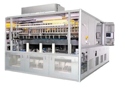 Laser repair equipment for TFT arrays (Bolite in partnership with Contrel Technology)
We've been working hard with our existing partners to develop additional laser solutions for mini & microLED applications and explore new opportunities in the solar and semiconductor industry in applications such as advanced packaging.
What experience do you have with actual microLED equipment? Have you had any sales into this market?
Yes, and with a global Tier 1 company no less! To date we already have about US$5 million in sales with that customer, with another US$10 million projected for 2022. Unfortunately, that's all I can disclose at this time.
Do you have experience in other fields of the emerging displays industry, like OLEDs or ePaper?
As a matter of fact, we do. We have recently been approached for a potential opportunity on laser repair of OLEDs. We are also working with another customer on a couple of laser microprocessing projects for ePaper application.
Anything else you would like to share with our readers and the industry?
microLED has the potential to revolutionize the display industry, and Bolite is very excited to hold the keys to some of the enabling technologies for volume production and market adoption. So, if you are interested in any of the laser applications mentioned, please reach out to us and discover what we are truly capable of!

