MicroLED inspection

Toray Research Center hosts an open webinar to discuss microLED display analysis and technologies

Toray Research Center (TRC) is hosting an open online webinar, with lectures focused on microLED displays and OLED materials analysis and evaluation. TRC, which supplies technical analysis and support for R&D and manufacturing, invites you to attend the online lectures at no cost to gain a deeper understanding of microLED technologies and the analysis of display devices. You can register to view the lectures here - note that the recordings will be available until June 1st.

The first lecture discusses new analytical technologies for morphology, structure and property evaluation. During the lecture, TRC researchers will discuss the center's In-Situ Heating TEM system, and how it enabled the reproduction and visualization of the bonding strength enhancement process induced by thermal treatment. Other topics in this lecture will include temperature- and humidity-controlled  nanoindentation measurements, AFM-IR for nanoscale functional-group and structural analysis, and the analysis of metal-organic complexes in liquid.

Read the full story Posted: May 12,2026

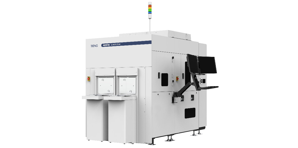
Semilab launches the LumiPix-3000 PL microLED inspection system

Semilab launched a new PL inspection system, the LumiPix-3000, with full wafer imaging capabilities designed for detecting intensity and wavelength defects in microLED devices.

Semilab says that its new system leverages advanced photoluminescence technology with multiple excitation options and high-resolution imaging to provide comprehensive defect analysis. It supports InGaN and AlInGaP materials on wafers up to 12 inches. Its non-destructive metrology approach enables the identification of various defects, including intensity variations, wavelength shifts, and morphological anomalies, based on the analysis of the captured PL images and other relevant data, while also fulfills industrial standards with its modern platform.

Read the full story Posted: Dec 03,2025

Alphabetter raises its Series A+ funding round, as it expands its microLED inspection systems globally

China-based microLED inspection systems developer AlphaBetter successfully finalized its Series A+ financing round, raising several hundred millions of Yuan (likely something between $30 to $100 million USD).

Several investor participated in the round, including GuoZhong Capital, AnXin Capital, Puhua Capital, Xiamen Financial Innovation, and Siming Science & Technology Innovation Fund. 

Read the full story Posted: Sep 28,2025

Instrument Systems: High Accuracy Optical Metrology for MicroLED Displays and Wafers

Author: Tobias Steinel, Steinel@instrumentsystems.com
Instrument Systems GmbH, Munich, Germany

Background

MicroLED (µLED) displays promise high contrast, fast response, wide color gamut, and long lifetime. However, production faces critical challenges:

  • Massive parallelization of testing: Millions of tiny µLEDs must be characterized quickly.
  • Metrology limitations: Narrow emission bandwidth and strong wavelength variability (≈5 nm) demand both speed and spectral accuracy.
  • Hardware requirements: In order to rapidly test and measure millions of µm sized µLEDs high resolution optics and cameras as well as precise detection algorithms are needed to avoid image artefacts due to low oversampling ratios (Rs).
Read the full story Posted: Sep 17,2025

Researchers develop a novel high-throughput and non-destructive microLED EL measurement technology

Researchers from China's Tianjin University has developed a high throughput and non-destructive EL measurement method for microLED chips. The researchers say that this new method is not only non-destructive, it also extends the lifetime of the probe significantly (to over a million contact cycles) compared to other methods.

The new method is based on a flexible three-dimensional probe array that is capable of adapting to the microscopic contours of micro-LED wafers. The total pressure applied on the LEDs is only 0.9 megapascals (said to be comparable to a gentle breath). The probe head has 32 × 32 pairs of probes that can simultaneously measure 1,024 microscale LEDs using a passive-matrix driving approach in half a second. 

Read the full story Posted: Jun 16,2025

JBD managed to dramatically increase its manufacturing quality, increasing yields and reducing defects

China-based MicroLED microdisplay developer Jade Bird Display announced that it has implemented new technologies that enabled it to reduce the average number of defective pixels in its microdisplays from around 100 to around 3 per panel. This increased the company's panel yields quite dramatically.

In addition to the improvement in defective pixels, the company also reduced the rate of its 'dark pixels' (which means pixels with reduced brightness) from around 0.4% a few years ago to only 0.03% today. This, in addition to the company's proprietary demura pixel-level luminance-compensation algorithm has greatly enhanced pixel-brightness uniformity.

Read the full story Posted: May 29,2025

The EL Advantage Over PL: Setting the Standard in microLED Testing

By: Dr. Tali Hurvitz, VP Research & Development & Noam Shapiro, VP Communications, InZiv

MicroLED technology  is transforming the world of displays, from AR/VR devices to cutting-edge automotive applications. However, in order for microLED to mature both technologically and commercially,  precise functional inspection continues to be essential. Photoluminescence (PL) and electroluminescence (EL) are two primary techniques for evaluating microLED functionality. PL testing measures light emitted from the microLED after excitation by a laser. This excitation mechanism causes a recombination across the entire junction (usually multiple quantum wells, depending on the excitation wavelength) which in turn leads to the emission of light. In this way, PL can measure certain basic properties of functionality.

IV (current-voltage) curve being measured during EL testing of a microLED chip

On the other hand, EL testing measures light emitted when voltage is applied to the LED, and in this case, the mechanism that activates the emission of light is the electrons and holes moving to the junction. Because electrons move much faster than holes, most electron-hole recombination—and thus light emission—occurs in the region of the junction where the holes are concentrated. This method of light excitation more accurately reflects real-world performance under operational conditions; the microLED display in the final electronic device will be activated via electric current and not via light.

Research has shown that EL is ultimately the superior method, and relying on PL alone, even while calibrating for inaccuracies, is an unreliable approach that often completely misidentifies defective LEDs as functional, and severely compromises measurement accuracy. Moreover, PL also often mischaracterizes the optical power and wavelength distribution across the wafer, failing to provide reliable testing results. We will briefly summarize below some of the research that has demonstrated the superiority of EL over PL for microLED testing and inspection.

Read the full story Posted: Mar 03,2025

InZiv Expands Management Team, Welcomes Dr. Tali Hurvitz as VP R&D

Israeli-based display inspection developer InZiv has recently expanded its management team, as the company reports increased interest in its microLED inspection systems. Dr. Tali Hurvitz has joined InZiv as its new R&D manager, bringing with her years of experience in the flat panel display industry and in the technology sector in general.

Dr. Tali Hurvitz earned her BSc, MSc, and PhD from Tel Aviv University, where she focused on physics and materials science. She has held significant positions, including her latest role as the Head of the Physics, Materials, and Innovation group at KLA, and has previously worked in various capacities within the technology sector. Dr. Tali will now lead InZiv’s R&D as the company matures and expands its solution portfolio.

Hello Dr. Tali, we first of all want to wish you the best of luck at InZiv. What drew you initially to the field of physics and materials science? 

As long as I remember myself, I preferred technical toys (like LEGO) to social ones (like dolls…). When in middle school I was directed to participate in cooking classes, while the boys went to study electronics - I rebelled and joined the boys! It was inspiring to learn how simple and straightforward electricity was. It is either zero or one. That led to my studying electronics in high school. My plan was to continue to higher education in that field as well. However, before starting my first year I took a preparation course in Physics - and I was hooked, till this day. Understanding the physical laws around us and forming these laws in simple equation - it's like magic!

Read the full story Posted: Sep 19,2024

A spotlight on Instrument Systems: a MicroLED Industry Association member

We're happy to interview Tobias Steinel Ph.D., works as a product manager at Instrument Systems GmbH, as part of our series of interviews with MicroLED Industry Association members. Germany based Instrument Systems manufacturers high-precision spectrometers, complex systems and software solutions for spectral light measurements.

Tobias is responsible for Instrument Systems’ measurement portfolio in the field of microLED optical testing and AR/VR/MR applications.

Can you please introduce your company and technology? 

With facilities in Munich and Berlin, Germany, Instrument Systems develops and produces high-end light measurement technology for flat panel displays, micro-displays, near-to-eye displays, automotive lighting, VCSEL systems and LED/SSL modules. Our color and light measurement solutions are used in display production sites worldwide. In addition to the manufacture of measuring equipment, our core competence is that our accredited test laboratory guarantees independent, reliable and comparable measurement results for every measuring device purchased. These can be traced back directly to the reference standards of national metrology institutes.


Read the full story Posted: Jul 10,2024

A spotlight on WEVE: a MicroLED Industry Association member

We're happy to introduce WEVE , a South Korean microLED inspection solution developer. The company collaborates with Korea’s largest display manufacturers, and is now approaching the global markets with its systems and solutions.

Can you introduce your company and technology?

WEVE is based in South Korea, and we specialize in Micro LED inspection solutions. Our technology is trusted by the biggest display manufacturers in Korea. We closely cooperate with industry-leading companies from Taiwan, Europe, and China. As a key technological partner of leading manufacturers, we have had to keep our operations out of the light for some time, which is why there is not much information about us available yet.

We do simultaneous AOI, PL, and Color difference analysis (xyY) of CoW, Epi-Wafers, and panels. We provide highly accurate, stable, and reliable solutions that can withstand high-volume inspections and the hardships of 24/7 heavy operations. I believe that WEVE is among the world's top companies by the total number of Micro LED wafers inspected thanks to our partners and customers who on one hand required us to keep things low but on the other, opened rare opportunities to sharpen our technology. Significant Inspection volumes provided valuable insights and experience needed to be at the frontier of the inspection field.

Read the full story Posted: Jun 25,2024