Aledia to setup a 140 million Euros GaN-On-Si microLED production line, start making microdisplay by 2022

France-based 3D GaN LED developer Aledia announced that it plans to establish a 140 million euros LED production fab in Champagnier, near Grenoble in France. The plan is to start LED production by 2022 - and by the company will also finalize its microdisplay production process and will start offering microLED microdisplays.

Aledia developed a microLED production process, based on a unique 3D architecture using GaN-on-silicon nanowires (branded as WireLED).
Read the full story Posted: Sep 14,2020

ALLOS and researchers from KAUST to develop high efficiency nitride-based red LEDs on silicon wafers

GaN-on-Si IP developer ALLOS Semiconductors announced it is collaborating with with Prof. Ohkawa and his team at King Abdullah University of Science and Technology (KAUST) to develop high efficiency nitride-based red LEDs on large diameter silicon substrates.

ALLOS and KAUST,nitride red LED on Silicon structure

Prof. Ohkawa and team have developed an indium gallium nitride (InGaN)- based red LED stack with low forward voltage of less than 2.5 V and high efficiency by using local strain compensation and a modified MOCVD reactor design. ALLOS and the KAUST team will combine their unique technologies to handle strain and optimize crystal growth conditions for GaN-on-Si and red LEDs. To this end, the KAUST team will grow its red LED stack on top of ALLOS's GaN-on-Si-buffer layers, which will be fine-tuned during the collaboration to optimize the performance of KAUST's red LED stack.

Read the full story Posted: Jul 21,2020

ALLOS Semiconductor sells its HPE and RF business, to focus on the microLED market

German-based GaN-on-Si developer ALLOS announced that it has sold its high-power electronics and RF business to AZUR SPACE. ALLOS will now focus its business on the microLED display market.

ALLOS Semiconductors developed its GaN-on-Si epiwafer technology for both high power electronics and Micro LED applications, but the time has come to focus on one market. The company says its 200 and 300 mm epiwafer technology is crucial in meeting the uniformity, crystal quality and manufacturability requirements of the novel Micro LED display applications.

Read the full story Posted: Jul 10,2020

ALLOS and Veeco up-scale GaN-on-Si microLED production technology to 300 mm wafers

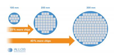
German-based GaN-on-Si developer ALLOS has applied its technology to large 300 mm epiwafers. ALLOS says that scaling up to 300 mm wafers enables higher production efficiencies and thus lower costs. ALLOS estimates that the higher area utilization alone accounts for a cost advantage of 40% compared to standard LED wafers. Standard 300 mm silicon line tools also offer higher production uniformity and yield.

Scaling up from 100 mm to 300 mm silicon wafers (ALLOS Semi)

ALLOS demonstrated the 300 mm scale-up using a reactor made by Veeco who announced selling the first 300 mm GaN reactor to a leading-edge semiconductor fab just some month ago and also showed 300 mm wafer data at CES. ALLOS reports a wavelength uniformity of consistently below 1 nm and "all other production requirements like bow of

Read the full story Posted: Apr 07,2020

Plessey and Compound Photonics to co-develop microLED microdisplays

UK-based GaN-On-Si MicroLED microdisplay developer Plessey Semiconductor announced that it has entered into a partnership with microdisplay system developer Compound Photonics to co-develop a Full-HD (1920x1080) 0.26-inch microLED display solution. The two companies expect to start offering samples in mid-year 2020 (not clear if these will be monochrome or full-color).

Plessey and Compound photonics, blue array microLED microdisplay photo

For this display system, Plessey will bond its micro-LED array wafer on Compound Photonics' backplane silicon wafer. The display module itself will be based on Compound Photonics’ NOVA digital drive architecture with MIPI input.

Read the full story Posted: Oct 18,2019

Plessey developed a 2.5-micron pitch MicroLED microdisplay

UK-based GaN-On-Si MicroLED microdisplay developer Plessey Semiconductor announced that it has developed a 2.5-micron pitch display, improving on its previous 8-micron pitch display it has demonstrated in May 2019 at SID DisplayWeek.

Plessey 2.5-micron pitch microLED microdisplay photo

The new display sports a 2000x2000 resolution and is a monochrome blue display. Plessey says that in early 2020 (during CES 2020, in fact) it will demonstrate a full RGB display on one wafer.

Read the full story Posted: Sep 23,2019

JBD demonstrates 2-million nits and 10,000 PPI Micro-LED microdisplays

Shanghai-based Micro-LED microdisplay developer JBD unveiled its latest Micro-LED microdisplay prototypes. JBD's panels can achieve a high brightness of 2 million nits coupled with very high pixel density (5,000 PPI) on a monochrome green display.

JBD also demonstrated an even high pixel density display (10,000 PPI). JBD can currently produce either monochrome or dual-color (red and green) microdisplays, and is developing full-color ones.

Read the full story Posted: Jun 23,2019

Plessey and JDC demonstrate a Full-HD monolithic micro-LED microdisplay

In 2018, UK-based GaN-on-Si MicroLED developer Plessey Semiconductor announced a strategic partnership with Taiwan's s Jasper Display Corp (JDC). Under the partnership, Plessey will use JDC's silicon backplane to drive its monolithic micro-LED displays.

Today JDC and Plessey demonstrated the world's first GaN-on-Silicon monolithic full-HD (1920x1080) microLED bonded display. Plessey says that it has succeeded in wafer level bonding of its GaN-on-Silicon monolithic microLED wafers with JDC’s eSP70 silicon patented backplane technology, resulting in microLED displays that contain addressable LEDs. The pixel pitch of this display is 8 microns and the JDC backplane provides independent 10-bit single color control of each pixel.

Read the full story Posted: May 14,2019

Plessey developed a process to produce native GaN-on-Si green micro-LEDs

UK-based GaN-on-Si MicroLED developer Plessey Semiconductor developed its proprietary 2D planar gallium nitride on silicon (GaN-on-Si) process to emit Green light without the need for color conversion techniques.

Plessey native GaN-on-Si green micro LEDs photo

Plessey says that its native Green LEDs are formed inherently using its proprietary GaN-on-Si epitaxial growth process similar to the native Blue LEDs with the principal difference coming in the amount of indium that is incorporated in the quantum well structures of the LED. The native Green emission is orders of magnitude times brighter than color-converted process for micro-LEDs.

Read the full story Posted: Mar 29,2019

Aledia orders more Micro-LED production equipment from Veeco

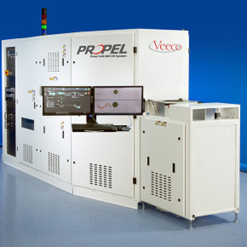
In July 2018, France-based 3D GaN LED developer Aledia announced that it has selected Veeco Instruments’s Propel GaN MOCVD system to support its advanced R&D. Veeco's Propel system enables Aledia to process 6- and 8-inch wafers or 2- to 4-inch wafers in a minibatch mode. Aledia also uses Veeco's R&D K465i MOCVD system.


Aledia and Veeco now announced that Aledia "expands its portfolio of Veeco equipment to develop and produce 3D micro-LEDs". It is not clear what kind of equipment Aledia ordered - and it also seems that the two companies are collaborating to develop next-generation Micro-LED production equipment.

Read the full story Posted: Mar 24,2019