HC Semitek installs the production equipment at its 6-inch microLED epiwafer fab in Jinwan
In August 2023, China-based HC Semitek started building its microLED epiwafer production line in Jinwan District, Zhuhai, China. The first phase of the $700 million microLED fab is expected to enter production by the end of 2024.

HC Semitek announced a few days ago that it has moved in and installed the production equipment in its new line. The company says it is on track to produce the first sample wafers in Q3 2024, and mass production is expected by the end of the year. The investment in the first phase will total $275 million USD.
ams Osram announces its new microLED strategy, will mostly withdraw from the microLED display market
In February 2024, ams-Osram announced that it's cornerstone customer (Apple) cancelled its microLED project, which will have dire implications for Osram's own $850 million 8-inch microLED epiwafer factory in Malaysia. Back then ams-Osram estimated that it will have impairment charges of $650 to $900 million and it will also likely to cancel or delay some of its investments in Malaysia.
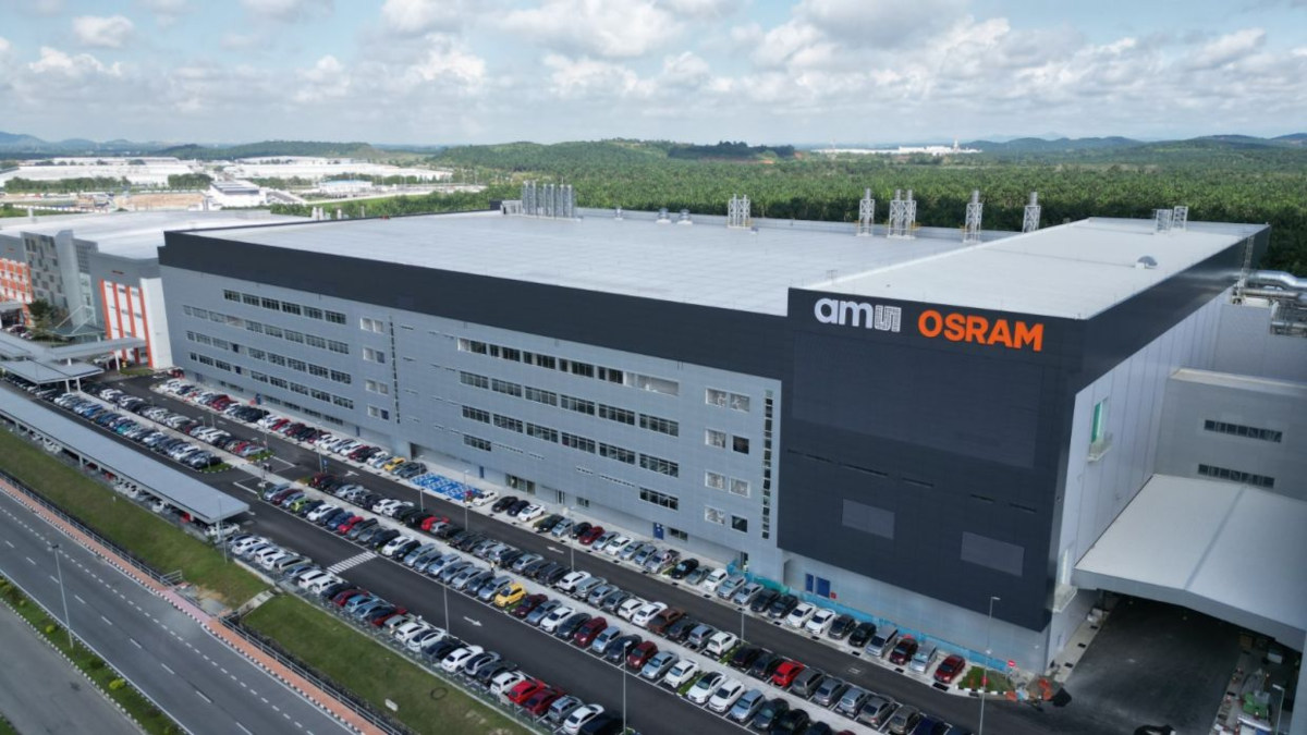
ams-Osram now announced its plans and strategy following Apple's decision to cancel its project. It seems as if the company has decided to pretty much withdraw from the microLED display market, and the only remaining microLED development efforts will focus on automotive lighting products. ams-Osram now believes that microLED displays will primarily play a role in several smaller applications that also will scale slower and later than previously expected. We also believe that microLED displays will take a longer time to mature than some in the industry have expected.
Aixtron reports strong momentum for MicroLED production systems
Aixtron reports strong results for its recent quarter, with both revenues and profit significantly higher than last year, driven by strong demand for SiC production systems for power electronics.
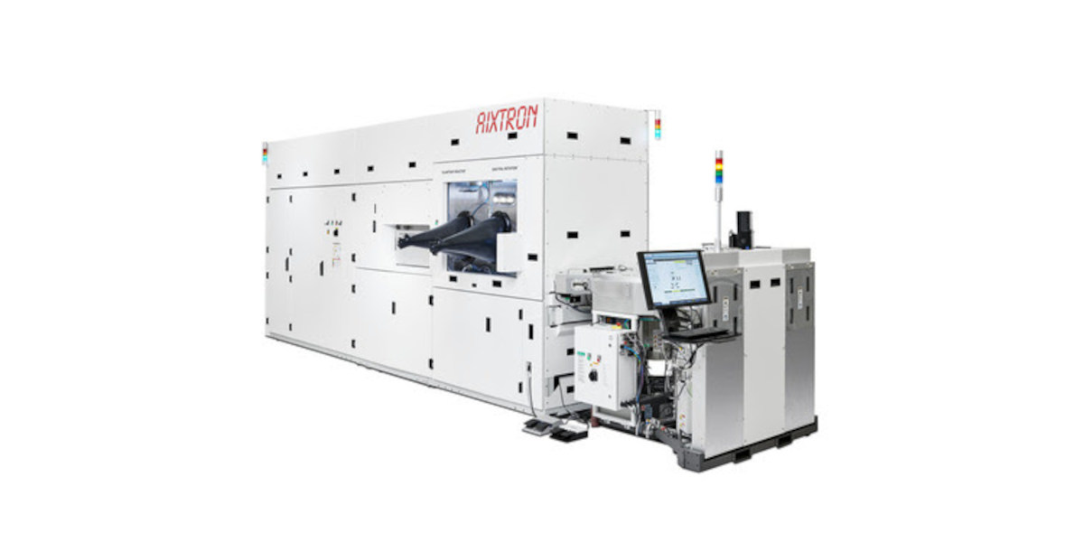
Aixtron reports revenues of 19.6 million Euro (up from 6.9 million last year) for LED and microLED systems. There's a strong new momentum for microLED production systems, which accounted for 37% of the equipment order intake. This development was boosted by the continued development activities of Micro LED customers, who are continuing to invest in development and pilot lines for the commercialization of Micro LED technology.
JBD starts shipping full-color RGB microLED microdisplay samples
China-based MicroLED microdisplay developer Jade Bird Display have started shipping engineering samples of single-panel RGB microLED microdisplays. The company brands these new microdisplays as the Phoenix series, while its monochrome panels are now branded as Hummingbird. The Phoenix series is designed to be used with 50+ degree FOV waveguides.
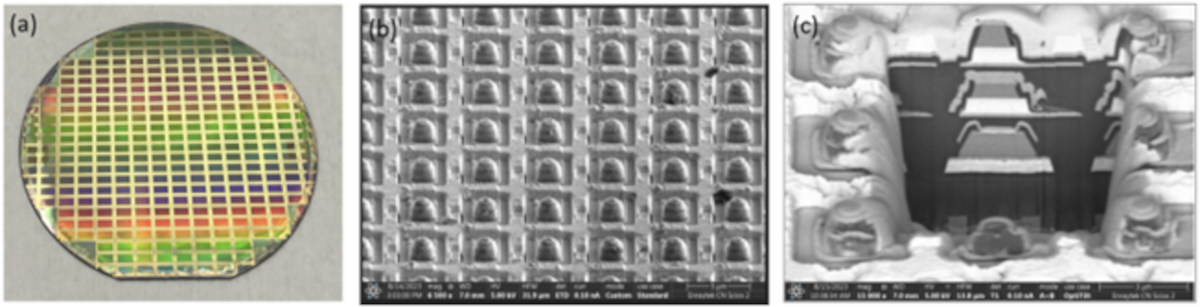
JBD's first Phoenix samples are 0.22" panels, with a 2K resolution (2.5 um pixel pitch). The three LEDs (RGB) are all AlInGaN emitters, and are vertically stacked. JBD says that its plans for a standard product include a 0.3-inch panel with 4K resolution (2 um sub-pixel pitch. The company expects to begin full mass production in 2025.
The MicroLED Industry Association to host an academic roundup webinar
On October 19th the MicroLED Industry Association will host a private academic roundup webinar, focused on the latest microLED research at leading academic institutes. During the webinar, we will hear from three world-class researchers that detail their latest projects and recent advances.

The webinar will feature three world-leading speakers, and will also be open to a Q&A session.
- Prof. Steven DenBaars, from the University of California, Santa Barbara (UCSB) – “Recent Advances in Micron Scale III-Nitrides based RGB MicroLEDs”
- Prof. Kei May LAU, from Hong Kong University of Science & Technology (HKUST) - (lecture topic TBD)
- Prof. Kazuhiro Ohkawa from the King Abdullah University of Science and Technology (KAUST) – “Highly efficient InGaN-based micro-LEDs”
IQE launches 200 mm RGB epitaxial microLED wafer products
Semiconductor wafer product supplier IQE launched a new portfolio of 200mm (8”) Red, Green and Blue epitaxial wafer products for microLED display qualification. The wafer epitaxy is based on GaN and GaAs materials.
IQE says that it plans to scale up its technology to 300 mm (12-inch) wafers, to enable more cost-effective solutions for microLED developers.
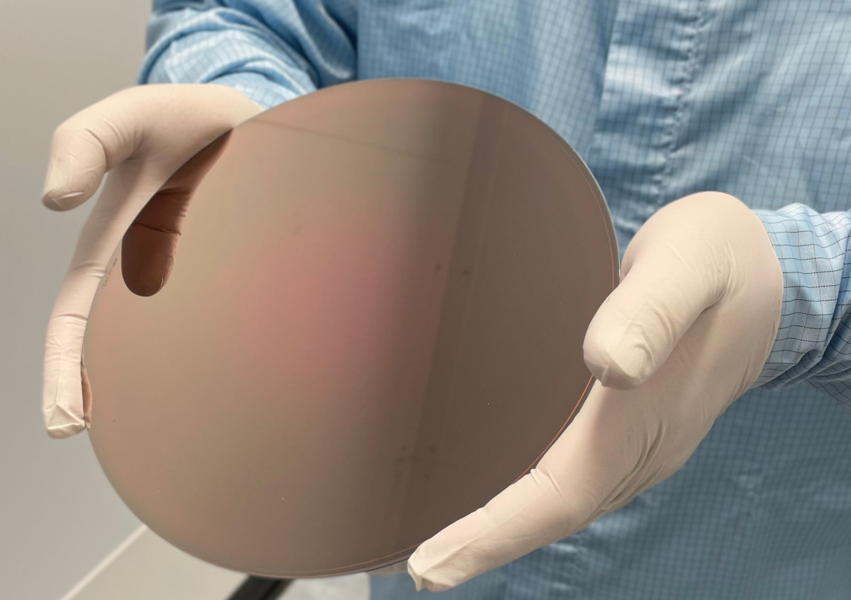
Mojo Vision lit up its first 300 mm GaN-On-Silicon blue microLED wafer
AR microLED microdisplay developer Mojo Vision announced that it has achieved a process milestone and has lit-up its first 300 mm GaN-on-Silicon blue microLED array wafer. The company says it is on track to maturing its 300 mm CMOS fab process.
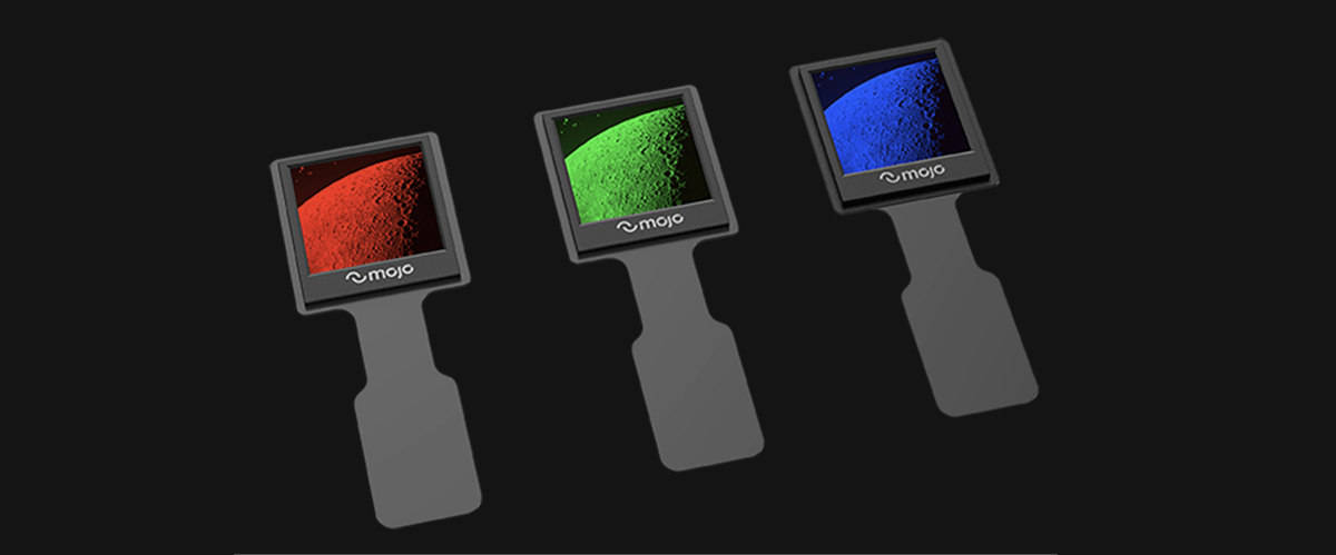
Mojo Vision is developing microdisplays based on blue LEDs and quantum dots color conversion. The company developed the world's highest density microLEDs, achieve up to 28,000 PPI (sub-micron LEDs).
A new report by Nikkei Asia details Apple's microLED production plans
Apple's microLED projects and goals have been reported and rumored many times in the past, and now the respected Nikkei Asia newspaper posted an interesting article with new details of Apple's microLED plans. Some parts of this plan were already published by other reporters, note.

According to the new report, Apple is aiming to get more involved in display manufacturing, to increase its control over its supply chain, and reduce its reliance on Samsung Display specifically. Apple has decided, therefore, to handle the LED transfer (pick-and-place) process by itself, at its R&D facilities in Longtan, Taoyuan, Taiwan.
InZiv launches an industrial-level high-speed wafer-level microLED inspection system
InZiv announced a new industrial-level microLED inspection system, called the REL. The company says that this new system provides unprecedented speed wafer-level EL testing of microLEDs. The REL system can rapidly obtain EL measurements on a microLED wafer, with up to 6 million LEDs in 1 hour.
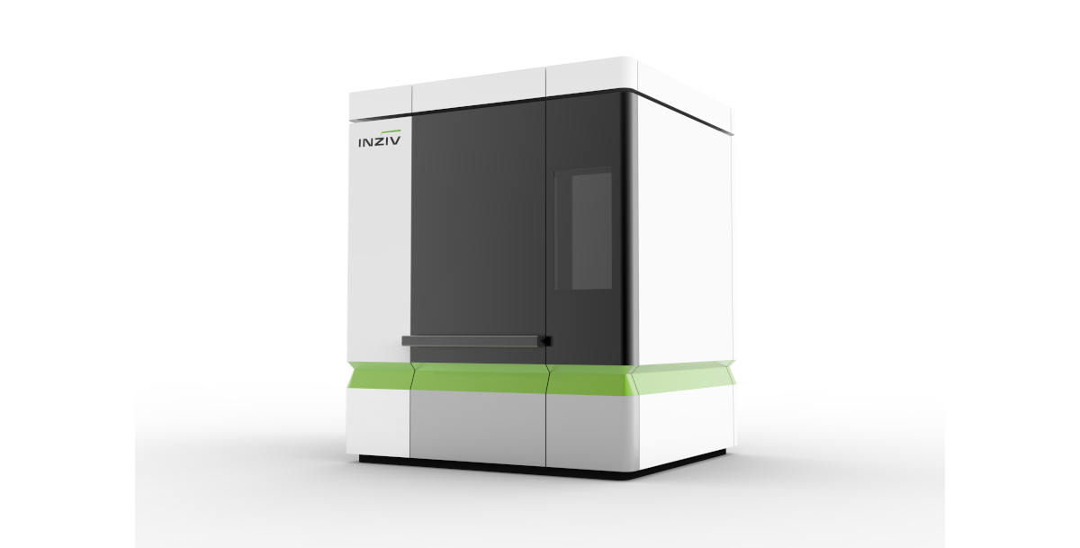
The company's unique technology offers repeatable, high- accuracy measurements, with no damage to the device. The system is fully compatible with both vertical and flip-chip designs. InZiv says that the REL offers the most critical and reliable microLED inspection on the market, enabling the advancement of all microLED applications. The company is already working on its next-generation system, which will double the output.
VueReal reports a major breakthrough in its microLED production technology
MicroLED developer VueReal says that it achieved a breakthrough in its MicroSolid Printing Platform, enabling it to go below 7um LED pitch (on the wafer) for full color microLED deposition. The company reports that its newest (and smallest) microLEDs show minimal impact on EQE, and this enables high-efficiency display production.
VueReal says that its new technology could soon compete on price with OLED displays while offering higher performance, and could be viable for many display segments - from wearables through smartphones to automotive and more. According to its current tests, its microLED displays will offer a brightness of 3,000 nits (and higher), while consuming around half the power compared to the latest AMOLED displays. In addition, its printing process is highly scalable and should not have a problem handling the demands of even the smartphone industry with hundreds of millions of displays per year.

