KAUST researchers develops highly-efficient GaN and InGaN red microLED devices

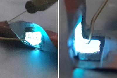
Researchers from King Abdullah's University of Science & Technology (KAUST) in Saudi Arabia developed GaN and InGan red microLED devices that are highly efficient.

The researchers managed to increase the efficiency of their previous design by a new chemical treatment that removes damages at the microLED sidewalls (created during the fabrication process) and also retains the high crystal quality at the InGaN and GaN sidewall interfaces.

Read the full story Posted: May 12,2021

Researchers use graphene to create detachable flexible microLED devices

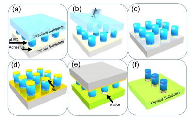
Researchers from the University of Texas at Dallas developed a new method to create highly flexible microLED chips, that can be folded and twisted. The LEDs are detachable, and can be attached to almost an surface.

Flexible MicroLED devices, University of Texas (September 2020)

The researchers used remote epitaxy, to grow the LED crystals on a sapphire crystal substrate, coated with a one-atom layer of 2D graphene, which prevents the LED to stick to the sapphire substrate.

Read the full story Posted: Sep 01,2020

Kyocera and OSRAM suggest hybrid PWM-current driving for microLED displays

Kyocera and OSRAM have jointly designed a new hybrid current and PWM driving technology for microLED displays. The two companies says that this new driving scheme can be used to avoid using lower pixel currents through microLED chips, which reduces the deviation of the luminance and the color shift at lower grayscale levels.

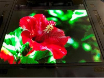
Kyocera and Osram: hybrid pwm/current driven 3.9-inch microLED prototype photo

Kyocera has presented a 3.9" full-color microLED display on an LTPS backplane that showed excellent performances that proves the validity of the new driving technology.


Read the full story Posted: Aug 11,2020

GE shows it is possible to inkjet print its red phosphor on plastic substrates

GE announced that it has been able to deposit its red phosphor (PFS-KSF) material using an inkjet printing process on a plastic substrate. This technology can be applied in future microLED and miniLED displays.

GE is also sampling a new green phosphor, that together with the red phosphor can attain 88% Rec. 2020. The company reveals that almost 40 billion LEDs with its PFS-KSF material were sold into commercial displays.

Read the full story Posted: Aug 06,2020

ALLOS and researchers from KAUST to develop high efficiency nitride-based red LEDs on silicon wafers

GaN-on-Si IP developer ALLOS Semiconductors announced it is collaborating with with Prof. Ohkawa and his team at King Abdullah University of Science and Technology (KAUST) to develop high efficiency nitride-based red LEDs on large diameter silicon substrates.

ALLOS and KAUST,nitride red LED on Silicon structure

Prof. Ohkawa and team have developed an indium gallium nitride (InGaN)- based red LED stack with low forward voltage of less than 2.5 V and high efficiency by using local strain compensation and a modified MOCVD reactor design. ALLOS and the KAUST team will combine their unique technologies to handle strain and optimize crystal growth conditions for GaN-on-Si and red LEDs. To this end, the KAUST team will grow its red LED stack on top of ALLOS's GaN-on-Si-buffer layers, which will be fine-tuned during the collaboration to optimize the performance of KAUST's red LED stack.

Read the full story Posted: Jul 21,2020

Researchers develop a new method to transfer and bond microLED arrays on flexible plastic substrates

Researchers from the University of Waterloo in Canada developed a new transfer and bonding method to deposit a flexible microLED array on plastic substrates.

Flexible microLED paste-and-cut technique schema, University of Waterloo

The technique, referred to as a "paste-and-cut", starts with temporarily bonding the LEDs on a process/handle wafer onto a glass substrate (the paste step). The LEDs are then released (cut) to the flexible substrate. This approach allows the LED to be optimized and then combined with other materials.

Read the full story Posted: Jul 11,2020

Sapphire nano-membranes enable higher-efficiency microLEDs

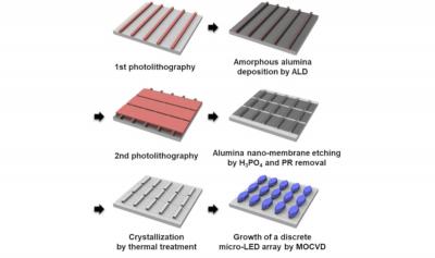
Researchers from Seoul National University (SNU) in collaboration with KAIST, SAIT and the Korea Photonics Institute developed a new method to deposit MicroLEDs on sapphire nano-membranes which enables chip singulation without an etching process. This method can enable higher efficiency MicroLED devices.

MicroLEDs grown on sapphire nano-membranes (SNU)

The researchers say that this method improves the internal quantum efficiency (IQE) of the microLEDs by 44% compared to standard GaN microLEDs produced on regular planar substrates. The microLEDs also featured a reduced dislocation density (by 59.6%). According to their tests, the microLEDs provided 3.3X the photoluminescence compared to regular microLEDs.

Read the full story Posted: May 11,2020

Researchers develop a new method to deposit high-brightness green InGaN microLED arrays

Researchers from the University of Sheffield a new fabrication process for green InGaN microLEDs that achieves high brightness compact microLED arrays.

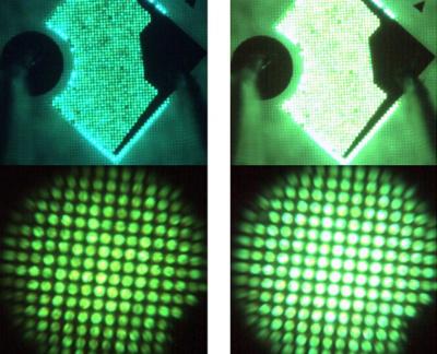
Emission microscopy of efficient InGaN green microLEDs (University of Sheffield)

Today most green InGaN microLEDs are produced by combining a standard photolithography technique with subsequent dry-etching processes on a standard III-nitride LED wafer. The researchers found a way to avoid the dry-etching processes which damage the surface the resulting LEDs. In the new process, the InGaN stack is direectly grown within pre-patterned micro-hole arrays through a thin (500nm) SiO2 layer serving as a GaN template over the epitaxial wafer.

Read the full story Posted: Jan 24,2020

The Perovskite Handbook - 2020 edition

MicroLED-Info and Perovskite-Info are happy to announce the 2020 edition of The Perovskite Handbook. This book is a comprehensive guide to perovskite materials, applications and industry, and it is now updated to January 2020 and lists recent developments and new companies, initiatives and research activities.

Perovskites are an exciting class of materials that feature a myriad of exciting properties. Perovskites are now entering the display market, with applications in quantum dots, LEDs, lasers and more.

The Perovskite Handbook

Reading this book, you'll learn all about:

  • Different perovskite materials, their properties and structure
  • How perovskites can be made, tuned and used
  • What kinds of applications perovskites are suitable for
  • Perovskites Quantum Dots
  • Perovskite solar cells, their merits and challenges
  • Perovskites-based LEDs
  • The state of the perovskite market, potential and future


Read the full story Posted: Jan 20,2020

iBeam Materials shows how to deposit both FETs and microLEDs directly on flexible metal foil substrates

iBeam Materials announced that it had successfully demonstrated the ability to produce high-performance GaN Field-Effect Transistors (FETs) directly on thin, flexible and rollable metal foil substrates.

This new technology complements iBeam's microLED deposition technology (demonstrated in the video above), and these FETs can be integrated with microLED chips in a side-by-side architecture. Both FETs and MicroLEDs are deposited on the flexible substrate without any transfer process.

Read the full story Posted: Jan 19,2020