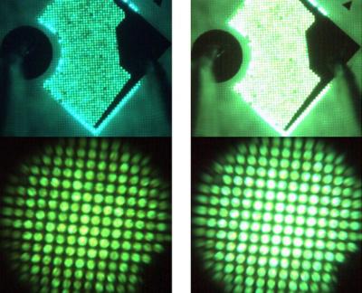
Researchers from the University of Sheffield a new fabrication process for green InGaN microLEDs that achieves high brightness compact microLED arrays.

Today most green InGaN microLEDs are produced by combining a standard photolithography technique with subsequent dry-etching processes on a standard III-nitride LED wafer. The researchers found a way to avoid the dry-etching processes which damage the surface the resulting LEDs. In the new process, the InGaN stack is direectly grown within pre-patterned micro-hole arrays through a thin (500nm) SiO2 layer serving as a GaN template over the epitaxial wafer.
The researchers use metalorganic vapour-phase epitaxy (MOVPE) to fabricate the individual microLEDs which are selectively overgrown within each micro-hole. The micro-hole masks offer a natural surface passivation around each microLED which can greatly simplify the device fabrication. All the μLEDs in the array share a common n-contact, while all the p-contacts are left open, which can then be contacted either individually or across large areas.
The researcher produced a few thousand 3.6 μm micro-LEDs, arrayed across a 0.1 mm2 surface and calculated that an individual 3.6 μm microLED could be brightly lit at an ultra-low driving current of 0.3 μA under a 2.5V bias. A 640x480 pixels display built around such LEDs would only draw 0.23W.

