KAIST researchers discover a way to create microLEDs that are not sensitive to sidewall defects
Researchers from Korea's KAIST have found that by changing the epitaxial structure of microLEDs, it is possible to fundamentally resolve the problem of efficiency degradation in microLED devices. In other words, it is possible to create microLEDs in which the efficiency does not drop with size.
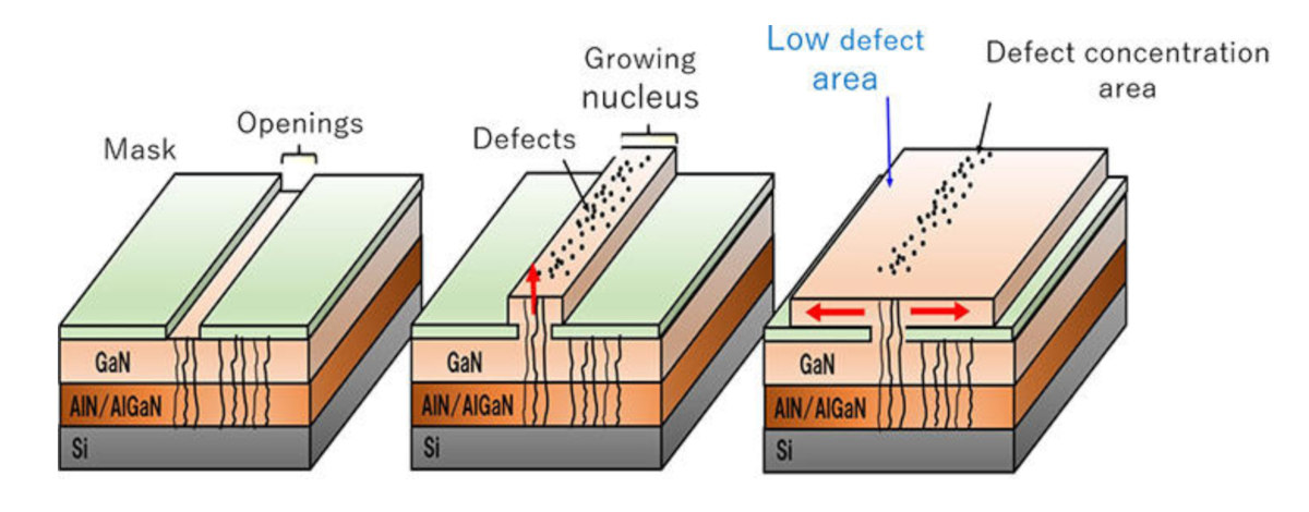
The researchers discovered that the specific epitaxial structure of the microLED changes how the current drives to the sidewall of the microLEDs. Based on that, the researchers developed a epitaxial structure that is not sensitive to sidewall defects. The proposed structure also reduces generated heat by about 40% compared to standard microLEDs.
Read the full story
Posted: Mar 27,2023