Kyocera Corporation announced that it has successfully developed a new process technology to produce microLED (and micro-laser) devices. The process is based on lateral growth of GaN layer on a silicon wafer, in a way that limits defects in most of the area.
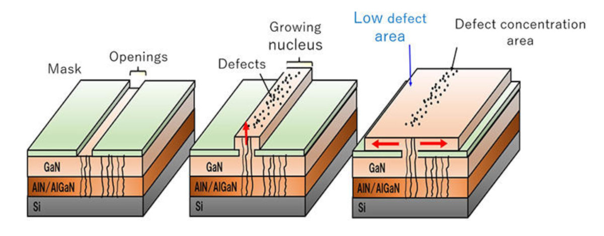
The basic process has three steps. First you grow a GaN layer on silicon. The second step is to apply a mask with a has a horizontal gap. The third step is to continue growing the GaN layer. The defects are concentrated in the opening nucleus, but the rest of the growth area remains almost defect free. The actual microLED devices are fabricated from the low-defect region.
Kyocera says that its new process has three main advantages. First is that the devices are made from low-defect GaN over wide areas, with consistent high quality. Second is that it is easy to pull the GaN devices out of the wafer, as the mask layer suppresses the bonding between the GaN and the Si substrate. Finally, the new method facilitates successful and reliable separation of the GaN device layer from the relatively inexpensive Si substrate, which will greatly reduce manufacturing costs.
