Technical / research

Researchers develop a femtosecond-laser based method of fine QD deposition for microLED color conversion display production

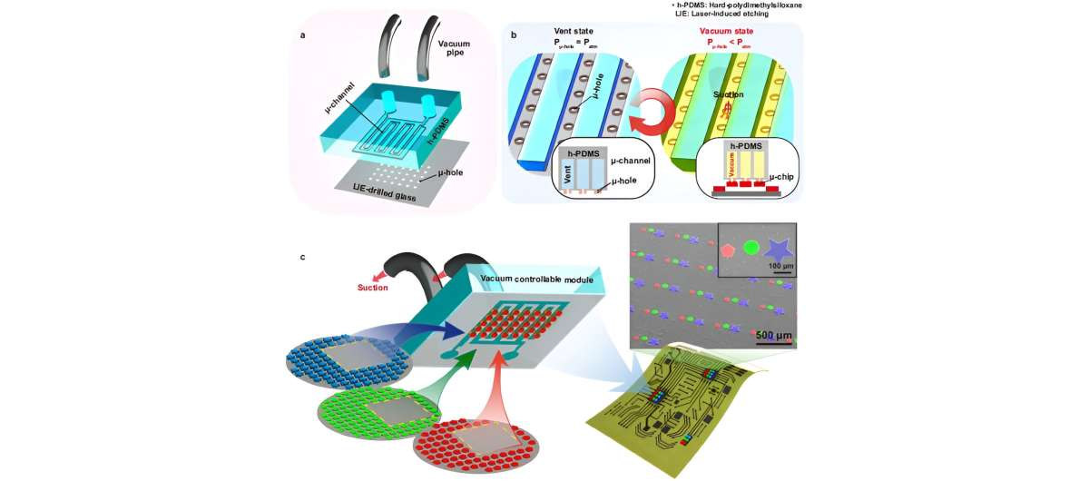
Researchers from the Beijing Institute of Technology developed a spatially shaped femtosecond-laser method for fabricating ultrafine quantum-dot pixels, that can be placed on top of microLEDs, for color-conversion display production. The method combines high-precision laser drilling with selective quantum-dot filling.

The process that the researchers developed starts with a glass substrate coated with a thin SU-8 polymer layer. A femtosecond laser was then used to drill ordered micro-hole arrays into the polymer. It is reported that the spatially shaped Bessel beam produced holes with clear entrances, smooth sidewalls, and low taper, with limited damage to the underlying glass. The holes can be as small as 100 nm.

Read the full story Posted: Sep 05,2026

Researchers develop transparent AlN resistive memory for grayscale control in microLED pixels

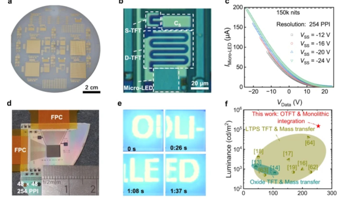
Researchers from Korea University, with colleagues from Shivaji University and Gyeongsang National University, have developed a transparent resistive memory device designed to drive individual microLED pixels, offering an alternative to the thin-film-transistor-and-capacitor circuits used in conventional active-matrix backplanes.

This research targets a persistent problem in transparent microLED displays, where the driving element must combine low off-state current, stable multilevel switching, and high optical transmittance. The researchers say that oxide-based transparent memories tend to exchange oxygen with the indium tin oxide (ITO) electrodes, producing high leakage and unstable switching, while nitride-based devices are more stable at the interface but usually switch abruptly between two states because of deep nitrogen-vacancy traps, making reliable grayscale operation difficult.

Read the full story Posted: Jul 02,2026

Researchers develop high-performance microLEDs on diamond substrates for optical I/O, launch Nexliumen to commercialize the technology

Researchers from China's Fudan University, in collaboration with researchers from Peking University, have developed high-performance microLED arrays, on diamond substrates, suitable for optical I/O.

The research combines several enabling technologies, including long-wavelength InGaN epitaxy, three-quantum-well active region design, diamond heterogeneous integration, transfer printing and two-photon fabricated microlenses. This resulted in highly efficient microLEDs, with very low drive currents and excellent energy efficiency. The researchers say that the diamond substrates effectively suppress self-heating, enabling high-speed operation while significantly improving thermal management compared with conventional glass substrates.

Read the full story Posted: Jun 28,2026

MTC and Hunan Normal University establish a microLED Optical I/O reserach center

Shenzhen-based MTC announced that together with the Future Technology Institute at Hunan Normal University, it is establishing a laboratory for microLED Co-Packaged Optics (CPO, or Optical I/O).

MTC says that the new lab will focus enhancing the communication performance of microLED devices and arrays, testing and validation, and prototype system design. This is applied research - MTC hopes to be ale to release sample products based on the lab research in 2027, with pilot production starting in 2028.

Read the full story Posted: Jun 16,2026

UCSB researchers developed a scalable monolithic transfer process based on selective electrochemical etching combined with wafer bonding

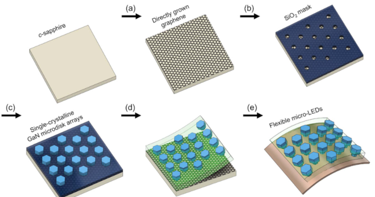
Researchers at UCSB developed a scalable monolithic transfer process that uses selective electrochemical etching of a highly doped GaN sacrificial layer combined with wafer bonding to release and transfer fully fabricated micro-LED arrays onto silicon in a single step.

The researchers report that this breakthrough process eliminates laser lift-off and serial pick-and-place transfer, enabling low-damage, high-throughput heterogeneous integration of microLEDs devices for displays, optical interconnects, and sensing.

Read the full story Posted: Jun 15,2026

Ingantec licenses strain-relaxed InGaN technology from the University of Wisconsin-Madison

US-based Ingantec announced an exclusive licensing agreement with the Wisconsin Alumni Research Foundation (WARF), for its patents in advanced strain engineering and the utilization of pseudo-substrates—technologies.

Ingantec says that the licensed IP, developed by University of Wisconsin-Madison Professors Shubhra Pasayat and Chirag Gupta, utilizes porosification and electrochemical etching techniques to create strain-relaxed Indium Gallium Nitride (InGaN) templates. Inagntec says that these methods may hold promises for solving the “green gap” problem —the precipitous drop in efficiency as InGaN based microLEDs move from blue to green and red.  

Read the full story Posted: May 20,2026

Researchers show that growing Eu-doped GaN LEDs on a semipolar crystal plane dramatically improves the red light emission

Researchers at the The University of Osaka, in collaboration with Ritsumeikan University have shown how growing europium-doped gallium nitride (Eu-doped GaN) on a semipolar crystal plane dramatically improves red light emission. 

Osaka University: Eu-doped GaN red LEDs

The researchers say that EU-doped GaN is a promising next-generation microLED material platform, as it provides narrow-linewidth, wavelength-stable red emission based on intra-4f-shell transitions of Eu ions. In this research, it was found that growing these on a semipolar crystal plane selectively promotes the formation of highly efficient Eu luminescent centers, resulting in red emission intensity more than 3.6 times higher than that of a conventionally grown material.

Read the full story Posted: May 13,2026

Researchers use machanical stretching to dynamically control the emission color of GaN LEDs

Scientists at the University of Hong Kong (HKU), led by Prof. Yang Lu, have successfully used mechanical stretching technology to dynamically control the emission color of GaN LEDs, from UV to blue light.

HUK GaN LED mechanically strainted - UV to blue

The researchers utilized micro-nano processing technology to fabricate single-crystalline GaN material into tiny bridge-like structures. Through precise mechanical stretching, the material achieved an elastic deformation of up to 6.8%, with a tensile strength of approximately 11 GPa. This demonstrates the extraordinary elastic deformation capability brought by the size effect, offering broad prospects for deep strain engineering.

Read the full story Posted: Apr 29,2026

Researchers combine dry/wet etching porcess with polymeric encapsulation to reduce microLED sidewall defects

Researchers from the University of Waterloo have demonstrated how a combined dry/wet etching process with polymeric encapsulation to construct InGaN-based microLEDs that show negligible degradation due to sidewall effects for devices having diameters as small as 6 µm.

The researchers report that the microLEDs exhibit low surface recombination velocities ( <10 cm s−1) and high wall plug efficiencies of 20.3% at a current density of 2.5A cm-2.

Read the full story Posted: Apr 22,2026