We're happy to interview Smartkem, as part of our series of interviews with MicroLED Industry Association members. UK based Smartkem developed a patented organic backplane display solution based on unique, patented inks. Smartkem's inks are solution deposited at a low temperature, on low-cost substrates to make organic thin-film transistor (OTFT) circuits.
Hello, can you introduce your company and technology?
Simon Ogier, Chief Technology Officer: SmartKem is a materials company that manufactures its unique and patented TRUFLEX® semiconductor and dielectric inks. These are used to make organic thin-film transistor (OTFT) backplanes for active matrix display driving. Our inks enable low temperature additive manufacturing processes that are compatible with existing a-Si TFT-LCD backplane equipment lines. SmartKem OTFTs have been used in emissive display backplane demonstrators achieving high brightness for microLED (>100K nits). The current stability under thermal bias stress testing is excellent and minimises threshold voltage shifts even under high current conditions. Our platform can be used in a several display technologies including microLED, miniLED and AMOLED displays for next generation televisions, laptops, AR and VR headsets, smartwatches and smartphones.
2. Can you say why you joined the microLED association and what it is you hope to achieve?
SmartKem joined the microLED association because we see our transistor technology being highly relevant for enabling microLED manufacturing in the next five years. The combination of high current driving abilities with the low process temperature allows the active matrix microLED device architecture to be turned upside down, manufacturing the LED array prior to the backplane. This changes quite fundamentally how the electrical connection is made between microLED and the driving transistors. Rather than having to form perfect eutectic metallic bonds to the millions of microscopic microLEDs, we can generate connections through the application of sputtered metallic contacts down via holes in planarization materials coated over the microLEDs. The transistor backplane is then processed at low temperature (<150ºC) on top of the planarized GaN LEDs, which is a low enough temperature so as not to damage them in any way.
SmartKem not only makes the OTFT materials but has also developed the planarization materials necessary to make the technology work.
3. What is your biggest challenge, and success to date in the microLED industry?
As a materials company, the biggest challenge for SmartKem is the generation of demonstrators of a low defectivity to illustrate the benefits of the chip first microLED manufacturing approach. We have access to R&D prototyping facilities in the United Kingdom that can help show a proof-of-principle, but to achieve perfect displays with millions of pixels and no lineouts or hot pixels is time consuming. Demonstration of the full potential of our approach requires partnership with companies with chip sorting and placement technologies. We are building these relationships actively and expect to be illustrating the progress over the coming months.
This year, Smartkem announced the creation of the world’s first monolithic microLED display using its OTFTs. Displays were made with 150K nits and 254ppi resolution, indicating a wide range of display formats could be driven using OTFT backplanes. Whilst this demonstration used LEDs still attached to the source wafer, it demonstrated the essential elements of high topographic planarization and subsequent OTFT matrix processing on top of microLEDs. Our next success will be showing that microLEDs deposited in a sparse array on a substrate can be processed similarly with OTFT to achieve the same display performance at a fraction of the cost compared with processing on the native GaN wafer.
4. Can you detail your latest prototype / demonstration?
The next prototypes we are working on will use sparse arrays of microLEDs to illustrate the benefits of the chip-first approach for creating high yield displays. The application will be for zonal backlighting of high resolution small-sized LCD but, once demonstrated, it should be possible to quickly move to larger area direct view RGB displays, and then eventually to monitor and TV applications.
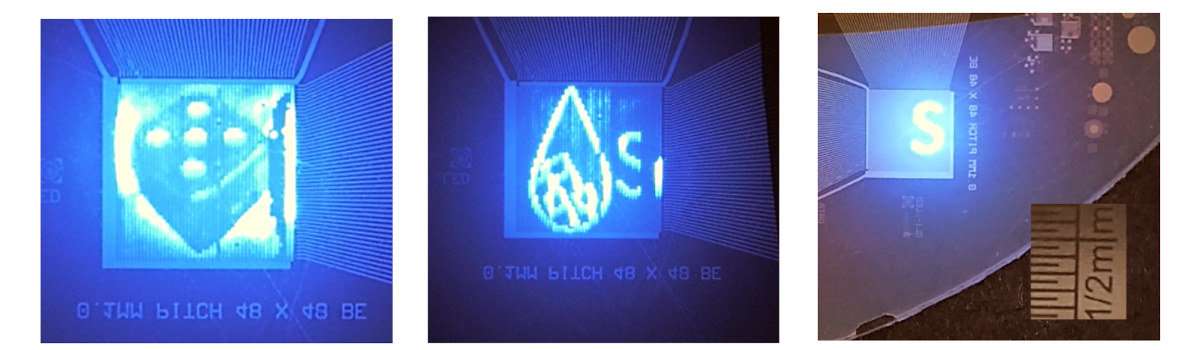
Still images taken from video sequences on the 254ppi monochrome 48x48 display (fine divisions in scale bar are 0.5 mm).
5. How do you see microLEDs changing the display industry in the next 5-10 years?
We are optimistic about the speed with which microLEDs can enter mainstream display applications. Using the chip-first approach is likely to be simpler than the current approach of soldering microscopic pads together, resulting in a higher yield. This is because it uses a conventional electrical via formation technique already established in mainstream manufacturing for display backplane. Once microLED displays are manufacturable at a reasonable price then displays will become more efficient and have a brighter appearance due to the highly efficient microLED technology. Both of these attributes have a particular benefit in battery powered devices such as smartwatches and mobile phones, so we can expect microLED to become the most preferred type of display with consumers.