Researchers from the US and Korea, led by MIT, developed full-color vertically-stacked microLEDs that achieve the highest array density (5100 PPI) and the smallest size (4 µm) reported to date.
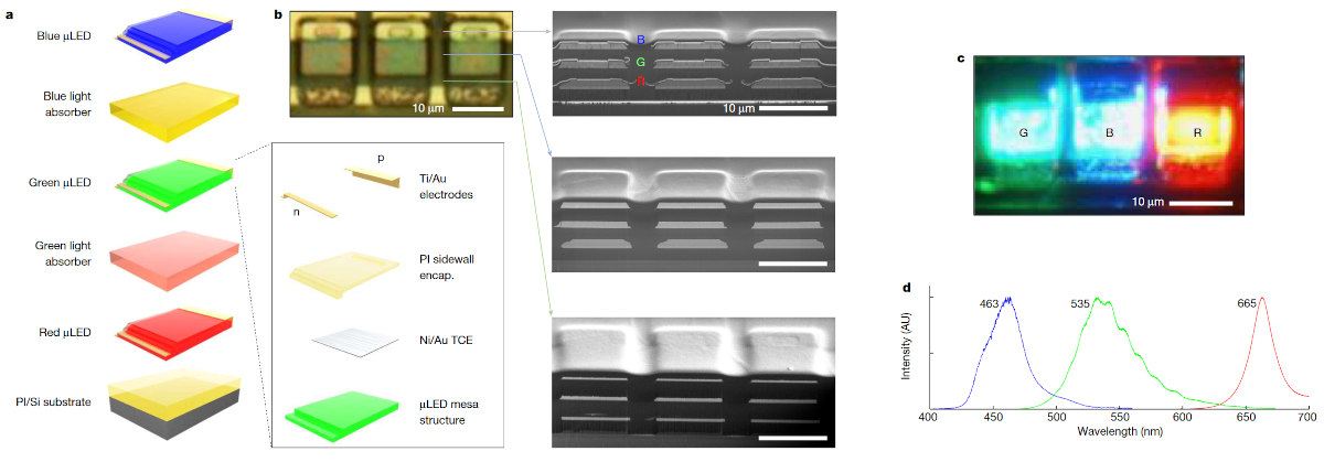
To end up with such high resolution and small microLED chip size, the researchers used a 2D materials based layer transfer (2DLT) technique. The resulting microLEDs, that have near-submicron thickness, are grown on 2D material-coated substrates, removed, and then stacked.
The researchers say that the smallest-ever stack height of around 9 µm is the key enabler for record high µLED array density. The researchers also demonstrated vertical integration of blue µLEDs with silicon membrane transistors for active matrix operation.
For the red AlGaAs-based LEDs, the researchers used graphene, coated on a GaAs wafer. For the InGaN-based green and blue LEDs, they used hBN on sapphire wafers. The graphene red LEDs were transferred using remote epitaxy, while the hBN blue and green ones were removed using Van der Waals epitaxy.
