300 mm

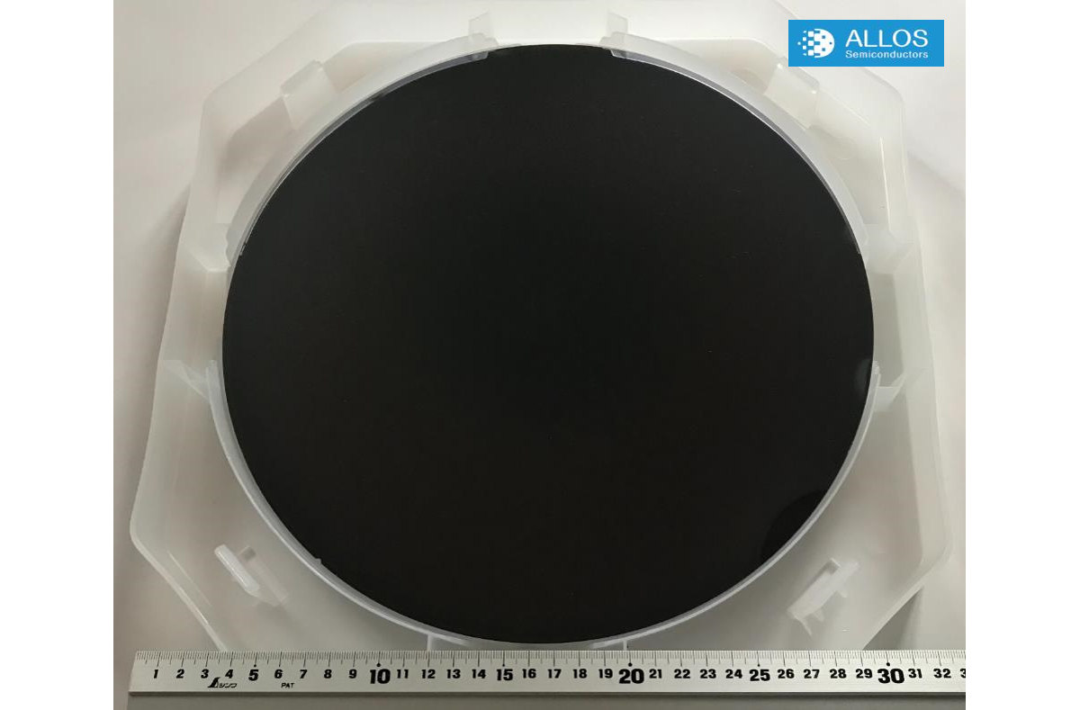
Mojo Vision lit up its first 300 mm GaN-On-Silicon blue microLED wafer

AR microLED microdisplay developer Mojo Vision announced that it has achieved a process milestone and has lit-up its first 300 mm GaN-on-Silicon blue microLED array wafer. The company says it is on track to maturing its 300 mm CMOS fab process.

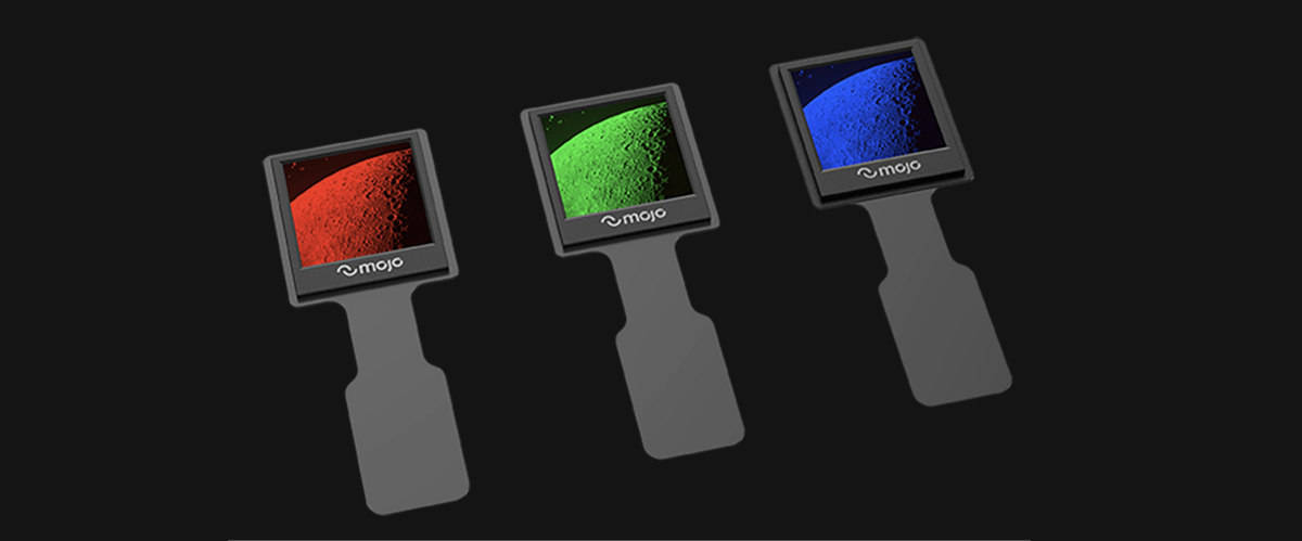
Mojo Vision is developing microdisplays based on blue LEDs and quantum dots color conversion. The company developed the world's highest density microLEDs, achieve up to 28,000 PPI (sub-micron LEDs).

Read the full story Posted: May 29,2023

Mojo Vision details its microLED microdisplay technology

Last month AR developer Mojo Vision announced that as it finds it challenging to raise more funds, it is changing its focus to develop its microLED display technology, and canceling its smart contact lens system R&D project.

A couple of years ago, Mojo Vision announced that it has developed a 14,000 PPI monochrome (green) microLED microdisplay, that is the world's highest density microdisplay. The company now updated its website, which says that its technology can reach up to 28,000 PPI.

Read the full story Posted: Feb 03,2023

Spotlight on ALLOS Semiconductors: a Microled Industry Association member

We're happy to interview ALLOS Semiconductors, as part of our new series of interviews with MicroLED Industry Association members. ALLOS Semiconductors is an IP licensing and technology company that focuses on GaN-on-Si technology for the microLED industry. ALLOS offers a turn-key technology transfer to establish a super-uniform CMOS-compatible large epiwafer process at customers within only 12 weeks.

Q: Hello! Can you introduce your company and technology?

ALLOS Semiconductors is the global leader for gallium nitride on silicon epiwafer technologies (GaN-on-Si) for next generation, micro LED-based display solutions and other applications building on more than 20 years track-record.

Our customer and partner base includes top-tier companies from the electronic device, display, LED and semiconductor foundry industries. They benefit from the cost, yield and performance advantages of our patent-protected 200 and 300 mm GaN-on-Si micro LED epiwafer technologies – including our unique 1 bin® technologies.

Read the full story Posted: Nov 07,2022

QustomDot and Aledia to co-develop full color microLED displays

QustomDot announced an agreement with France-based 3D GaN LED developer Aledia to co-develop a full-color microLED displays, based on Aledia's high-efficiency Gan-on-Silicon 3D Nanowire LEDs grown on 300 mm wafers coupled with QustomDot's high performance quantum dots color conversion technology.

Aledia microLED produced on 300mm silicon at CEA-Leti

QustomDot developed a patented method to produce high-quality and stable QD materials suitable for microLEDs, that are heavy metal free. A few months ago the company announced it is co-developing microLED displays with MICLEDI.

Read the full story Posted: Oct 25,2022

MICLEDI to develop red microLED AR displays in collaboration with IQE

Belgium-based microLED microdisplay developer MICLEDI announced a partnership with IQEa supplier of compound semiconductor wafer products and advanced material solutions to the global semiconductor industry, to develop microLEDs for AR products.

Under this agreement, IQE will provide MICLEDI with a 200mm (8-inch) platform to scale and commercialise its technology to achieve high-volume production for red microLEDs. This geometry allows for compatibility with both standard 200 mm and 300mm silicon foundries, which enables the partnership to deliver economies of scale.

Read the full story Posted: Oct 06,2022

Enkris launches GaN-on-Si microLED epiwafers on 300 mm wafers

China-based GaN epiwafer producer Enkris Semiconductor launched new microLED epiwafers. The "Full Color GaN" series offers GaN-on-Si microLED epiwafers, with wafers sizes of up to 300 mm.

Enkris full-color GaN microLEDs series

Enkris' new epiwafers offers blue, red and green LED arrays, all based on the same material platform. Enkris Semiconductor uses its patented strain engineering and polarization engineering, which it says is unique, to expand its GaN-on-Si LED epiwafer product portfolio to all colors (with wavelengths of 390-650nm).

Read the full story Posted: Apr 11,2022

MicroLED microdisplay developer MICLEDI raised 7.1 million Euro

Belgium-based microLED microdisplay developer MICLEDI announced that it has raised 7 million Euro from FPIM and KBC Focus Fund. The funds will enable the company to transition from the pilot line technology development to product design and subsequently to the manufacturing phase.

MICLEDI's team at imec

MICLEDI reveals that its next steps will be to demonstrate its native-RGB microLED display on 300 mm wafers, prepare its technology IP for transfer to a foundry partner for manufacturing and launch its product development phase.

Read the full story Posted: Mar 04,2021

STRATACACHE CEO details the challenges and goals of the company's upcoming US-based microLED display production fab

Global digital signage solution provider STRATACACHE is constructing the first US-based complete display production facility in Eugene, Oregon. The future MicroLED E4 fab is planned to commence production in 2022, and the fab will be a complete microLED production line, from epiwafer (on 300 mm silicon wafers), through transfer process and to final module assembly.

STRATACACHE Eugene E4 MicroLED fab photo

This project is extremely interesting, and we set out to discuss it with STRATACACHE's founder and CEO, Chris Riegel. At STRATACACHE, Chris leads strategic direction, technology development and engineering operations, and the MicroLED fab project seems to be personally spearheaded by him.

Read the full story Posted: Feb 27,2021