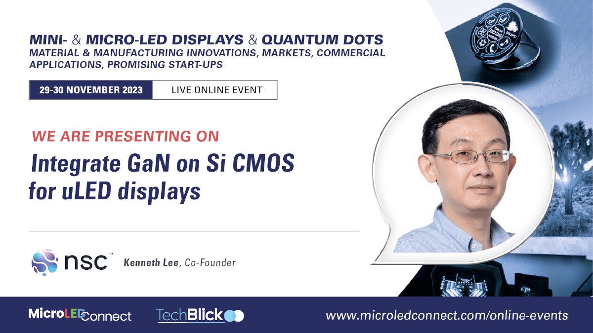
Singapore-based nsc innovation is an integrated circuit design company, that develops microLED microdisplays based on a monolithically integrated silicon CMOS with GaN LEDs platform, produced at full wafer scale. Kenneth Lee, nsc's co-founder, will give a lecture at the upcoming MicroLED-Connect virtual webinar on November 2023, and was kind enough to answer a few questions we had.
Hello Kenneth, can you give us a short introduction to nsc and your microLED technology?
nsc is an integrated circuit design company based out of Singapore. nsc aims to enhance the human experience through future technology by creating ground-breaking integrated circuits that will underpin future technological waves.
Our chips are the first to effectively integrate silicon CMOS with GaN LEDs monolithically and at full wafer scale, while maintaining compatibility with traditional CMOS manufacturing. By doing so, nsc offers the functionality and manufacturability needed to enable widespread adoption of microdisplays.
Our chips’ end products are applicable across multiple technology sectors including illumination, AR / VR Displays and 5G / 6G connectivity.
What will you talk about during the microLED Connect's event?
We will present our recent progress in developing a scalable and cost effective 200 mm manufacturing pathway for integrated CMOS + GaN LED single chip solutions for microdisplay applications. This will include a detailed description of the advantages of front-end CMOS/III-V integration to avoid challenges in packaging and tight contact pitch wafer bonding approaches.
What do you think are the main challenges in the MicroLED Industry today?
The main barrier in the adoption of GaN-based microdisplays are the yield and cost issues associated with chip-level advanced packaging solutions. These yield challenges drive costs to levels which are not amenable for consumer technologies. A low-cost and high-yield manufacturing pathway must be established to reach these stringent cost targets.
What market segments do you feel will be the first to adopt MicroLEDs?
The markets which will adopt MicroLEDs first are on both ends of the display segment. In the small form factor (i.e. microdisplay) space, premium AR glasses will begin adoption of microdisplay projectors and become more mainstream when the capabilities of these AR glasses improve. In the larger form factor space, applications with a lower total number of pixels (i.e. smart watch/wearables) are most likely to see early adoption due to the reduced manufacturing complexity and a greater ability to control repair/replace costs. Beyond that, higher margin or hidden margin products such as high-end consumer TVs will be next due to a greater ability to absorb higher manufacturing costs/yield challenges.
Which next-gen technologies do you think are most promising for the future of the MicroLED display industry?
We believe that front end integration of GaN LEDs with CMOS backplanes provides a unique a pathway to high yield manufacturing by leveraging the manufacturing quality and high interconnect density benefits of CMOS foundries and avoiding challenges with advanced packaging solutions. We feel that this can revolutionize the microdisplay manufacturing process and lead to costs and yields which are amenable to consumer applications.
Thank you Kenneth, looking forward to hearing your lecture in November!