This is a sponsored post by Applied Materials
Applied Materials Baccini Cell Systems provides advanced screen-printing solutions and systems for a wide range of applications - including for MicroLED production.
Here is an interview we conducted with Applied Materials' Director of Global Product Marketing, Daniel Hada, who details the company's solutions for MicroLED production and R&D.
Q: Can you tell us a little bit about Applied Materials' Baccini systems? What kind of systems are you offering?
We provide advanced screen-printing solutions for both R&D applications and high volume manufacturing. All Baccini systems are built for sheet-to-sheet printing, either on flexible or rigid substrates. In addition to our screen-printing capabilities, we also provide customers with different drying and curing solutions, in-line inspection systems to monitor the quality of the print immediately after the print, and fully automated print lines to enable low cost, and high volume manufacturing. Utilizing Baccini’s Esatto technology which provides high accuracy and high print repeatability, we developed the Double Print technology years ago, to allow print on print capability for printing narrow lines/small features with high aspect ratios and to minimize interruptions in the printed lines.
For R&D, we can provide systems with manual load and manual unload, or with automatic load and unload of substrates. The R&D systems can be stand-alone printers or be combined with loader and unloader, with or without drying ovens. Our R&D systems are also capable of high accuracy and high print repeatability and can be eventually retrofitted and upgraded to a pilot line production system.

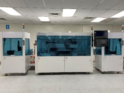
Fig. 1 Tempo Presto PE, Applied’ platform for microLED and general PE applications
Q: Applied says that over 50% of all solar panels were produced in part using Baccini systems' printers. What enables this resounding market success?
This accomplishment is a prime example of listening to our customers and providing solutions to address their high value problems. This is also an example of our longevity in the solar industry, which goes back to our first Rotary Line production system in the early 1990s. Since then, we have developed new capabilities to improve throughput and printing quality, reduce wafer breakages (note that solar wafers are very brittle, unlike semiconductor wafers or substrates used in printed electronics) and improve yield, while wafers have gotten larger and thinner. This success also demonstrates the commitment our customers have made to continue to purchase Baccini screen-printer lines and the value they see in our technical capabilities.
Q: What kind of solutions can you enable for MicroLED display developers?
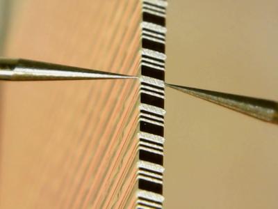
Over the years, we have developed several screen printable solutions for uLED applications. Our key innovation allows our customers to screen print the edge electrode, otherwise known as the wrap around electrode. Our technology allows our customers to print fine lines on the front, back and edge of the substrate, forming conductive lines from pads on the front of the substrate to corresponding pads on the back of the substrate. Our additive screen print solution provides a single step and cost effective alternative to expensive sputtering processes requiring multiple process steps such as masking, patterning, sputter and mask removal.
Our first engagement for uLED was for the bondpad application. For this application, we printed solder paste on predefined pads across the substrate for subsequent placement of the LEDs. Screen printing provides two key advantages for this application: fast printing speed since the entire substrate can be printed within seconds and repeatability of the print pattern since the opening pattern of the screen will remain stable through 1000’s of prints. In all honesty, screen printing for uLED bondpads may be suitable for miniLED and early generation uLED designs but may run into difficulties once the uLED shrink to very small geometries. Solder paste or other types of conductive adhesives contain particles which will need to shrink significantly to keep up with the shrinking uLEDs. If this does not happen, then alternative techniques may be required in the future. Of course, we are keeping track of our customer’s roadmaps and will continue to improve our capabilities for this application.
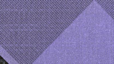
Customers have also used our screen printers to print the conductive circuits on the back side of the frontplane to apply power to the uLEDs. For this application, high density lines are printed, often with the line and space ratio less than one (for example, 60um wide lines with 40um spacing between the lines). As with the edge electrode application, screen printing is a high throughput, low cost alternative to the next best alternative (typically sputtering).

Fig. 2 Wrapped around electrode, minimum Line/Spacing 60/40 um
Q: We understand that die attach, the basic step for microLED bonding, can be done using your printers. What is the advantages of using screen printing for this step compared to other methods?
Screen-printing for the bond pad application brings a couple of distinct advantages compared to alternate deposition techniques. Screen-printing in general is a very fast deposition technique, allowing full area coverage in a very short time. Our printers are capable of print speeds up to 1000 mm/s, which means a 200 mm substrate can be printed in a little more than 0.2 seconds. Of course, the printing speed needs to be optimized between the pattern to be printed, the feature size and the material to be printed (amongst other things). Compared to other print techniques, however, the speed to print entire substrates, whether a blanket film or a patterned print (like the bond pad print) is significantly faster with screen printing than with other techniques like inkjet, jet dispense, etc.
The other advantage with screen-printing for this application is the alignment accuracy and the repeatability of the print pattern. For high alignment accuracy applications, our customers use our Esatto technology, to ensure print alignment down to ±5um. Screen-printing pattern repeatability is a function of the consistency of the print process, combined with the deformation of the screen or stencil and the homogeneity of the paste material. From an equipment perspective, our screen-printers are known for the consistency of the print process; for applications like bond pad, we use stencils with minimal deformation; and we work continuously with our material partners to develop materials that can be printed consistently over long periods of time. As a total solution, we believe our screen-printing solution gives our customers the best opportunity for success while achieving very high productivity.
Q: The screen printing machines can also be used to deposit very fine conductive lines. Where are these conductive paths required in microLED displays? When producers make seamlessly tiled microLED displays, there's a need for complicated conductives. One solution is side wiring - and here screen printing can be very effective, can you give us more details?
As we discussed before, the fine lines for uLED can be used to print the edge electrode (aka wrap around electrode or side wiring) and/or to print the conductive circuits on the TFT panels. For these applications, the main requirements of our customers are: high conductivity (>50% Ag bulk), relatively high thickness (3 to 10 μm), proper adhesion to the substrate and low linewidth (

Fig. 3 Fine lines printing, Line/Spacing 60/40 um
Q: Via paths is another technique that can be used to connect tiled microLED displays. What are the advantages and disadvantages of VIA filling compared to side wiring? Will VIA paths be the next-generation solution?
Some of our customers have asked us to demonstrate via fill with aspect ratios as high as 10:1 with via diameters as small as 40um. By moving the conductive lines from the edge of the substrate to the middle of the substrate, display makers will be able to realize true bezel-less display tiles. Via fill also allows the uLED density to be increased since the conductive lines will be going through the substrate as opposed to wrapping along the edge of the substrate where area for the conductive lines are constrained.
This technology is still in R&D, as many aspects of this solution are still being improved. Costs and yield for the creation of the via opening need to be improved and the process flow to create the vias need to be optimized. The conductive materials for filling the via needs to be improved to achieve high aspect ratio fills with continuous conductive paths. After the print, inspection systems to verify acceptable filling of the via needs to be developed while the speed of inspection will need to meet the throughput requirements for high volume manufacturing. Different types of printing techniques are also being improved to demonstrate current capabilities, but also to demonstrate future or roadmap requirements. From the Applied Materials’ perspective, we have been able to demonstrate via fill for a number of different geometries in R&D for our customers but beyond that, high volume performance has not been demonstrated due to a lack of test substrate.
Q: How does Applied Materials see the future microLED market? Do you already see demand for industrial production or is that too early?
Within Applied Materials, we have many people and groups working on different value chains within the Display market and microLED is one of those areas where we are extending great focus. From the Baccini perspective, we see great interest from our customers to leverage the simplicity, flexibility and cost advantages of screen-printing relative to the alternative technologies, to significantly reduce the overall costs and simplify the manufacturing of uLED displays. The industry recognizes the current costs to manufacture microLED needs to be reduced significantly in order to stimulate wide customer adoption regardless of the improved display characteristics. Besides cost reduction, microLED display makers are also focused on developing new technologies to place the microLEDs onto the substrates. This has been an area of development for several years.
Until these issues can be addressed, microLED will be an interesting new technology with many advanced capabilities, but with a relatively small market. In general, we see the market adoption is still relatively low, and most of our customers can supply their products without large scale production capabilities. Once the market requires high volume production of microLED Displays, our Tempo Presto PE screen print system is the ideal system to meet their production requirements. Until then, microLED may initially be a niche market, using those opportunities to improve manufacturability and reduce costs, before moving into the highly competitive consumer display applications.
Q: We understand Applied can support screen printing at R&D settings, and also at a fully industrial scale. What are the key value points of Applied's screen printing technology and total solution capability?
Our team at Applied Materials Baccini take great pride in our screen printing history, and in the capabilities and commitment of our technology team and in the strong partnerships we have developed across the screen printing value chain. Over the years, as our customers challenge us with requests to print on larger and thinner substrates, we have responded by developing systems of increasingly higher throughput, starting with single lane systems that printed 1440 wafers per hour on 125x125 mm wafers, our latest generation dual lanes systems print up to 8000 wafers per hour on substrates up to 166x mm, or over 7000 wafers per hour on substrates up to 210x210 mm. For all of our systems, we provide several dryer options, enabling our customers to chose different drying solutions depending on the requirements of their pastes.
In addition to these productivity improvements, we are constantly developing new capabilities to improve print quality and to reduce costs to our screen-printing customers. With our newest printer platform, we are now able to achieve print alignment repeatability of ±5um in HVM. Combined with our proprietary Double Print technology, we are able to print small features very accurately at high aspect ratio and/or to print fine lines at high aspect ratio with lowered risk of line interruptions. To ensure the print quality, our Esatto AOI (post print inspection) capability can be added to our printer modules to perform inspection of the printed pattern immediately after the print. Print defects can be detected immediately after the print is completed. Other innovations that have been implemented on our systems include an automated screen cleaner, auto scales to weigh the paste laydown on a substrate (before and after print), capability to predict screen failure before breakage, to name a few of our enhancements which may be valuable to our customers.
Lastly, all Baccini platforms are compliant with the latest Industry 4.0 requirements: our proposal is a software tool embedded in the screen printing line to perform data collection and data management such as historicization, tagging and KPI (Key Performance Indicators) calculation. On top of the this, multiple software features can be added with machine learning algorithms to optimize recipe tuning, implement closed-loop controls and predictive maintenance, thus increasing uptime and yield and reducing the need for highly skilled operators.
For new engagements with our Printed Electronics customers, our dedicated process engineers in our R&D group work with each of our customers to demonstrate our capabilities specifically to address customer requirements. We work with our suppliers to design and develop the correct screen (or stencil), choose the correct paste or ink, then using our customer’s substrates, perform the necessary print optimizations to meet customer requirements. Since many of our Printed Electronics customers do not have a strong background in screen-printing, our goal is to provide our customers with a total solution, comprising of the proper screen design, the optimized material and the best screen-printing equipment solution. Using the processes we develop in R&D, we can transfer the process onto our production system, and by providing our customers different equipment options, our customer’s time to market can be significantly reduced.
For more information on Applied Baccini's microLED system click here or contact the Baccini team here - printed_electronics@amat.com