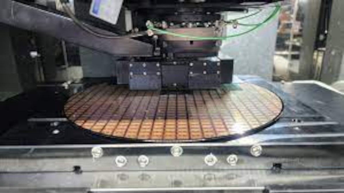
Researchers from Korea's ETRI institute developed a new chip packaging material, that is said to reduce the power consumption of the process by 95%, and reduce the number of required stages from 8 to 3. This could make semiconductors production much more efficient and lower in cost.
The technology is applicable to all high-end semiconductor production - including microLED production. Indeed the team reports that they have reached out to several microLED developers to evaluate the technology, and the initial testing has been very positive. The material could be commercialized in three years.
The base technology in this achievement is a new non-conductive film technology, based on a polymer film made of epoxy-based substances and a reducing agent, with a thickness ranging from 10 to 20 micrometers. This material has been under development for almost 20 years.
The three steps in the new chiplet packaging technology is applying the NCF film on the wafer, irradiating it into chiplets using a laser and finally hardening the resulting 'tiles'.

