The microLED transfer process is crucial in MicroLED display production, this is likely to be the most challenging part of the entire process. In this article (an excerpt from The MicroLED Transfer Process Report), we'll give an overview of the transfer process, its challenges, and alternatives.

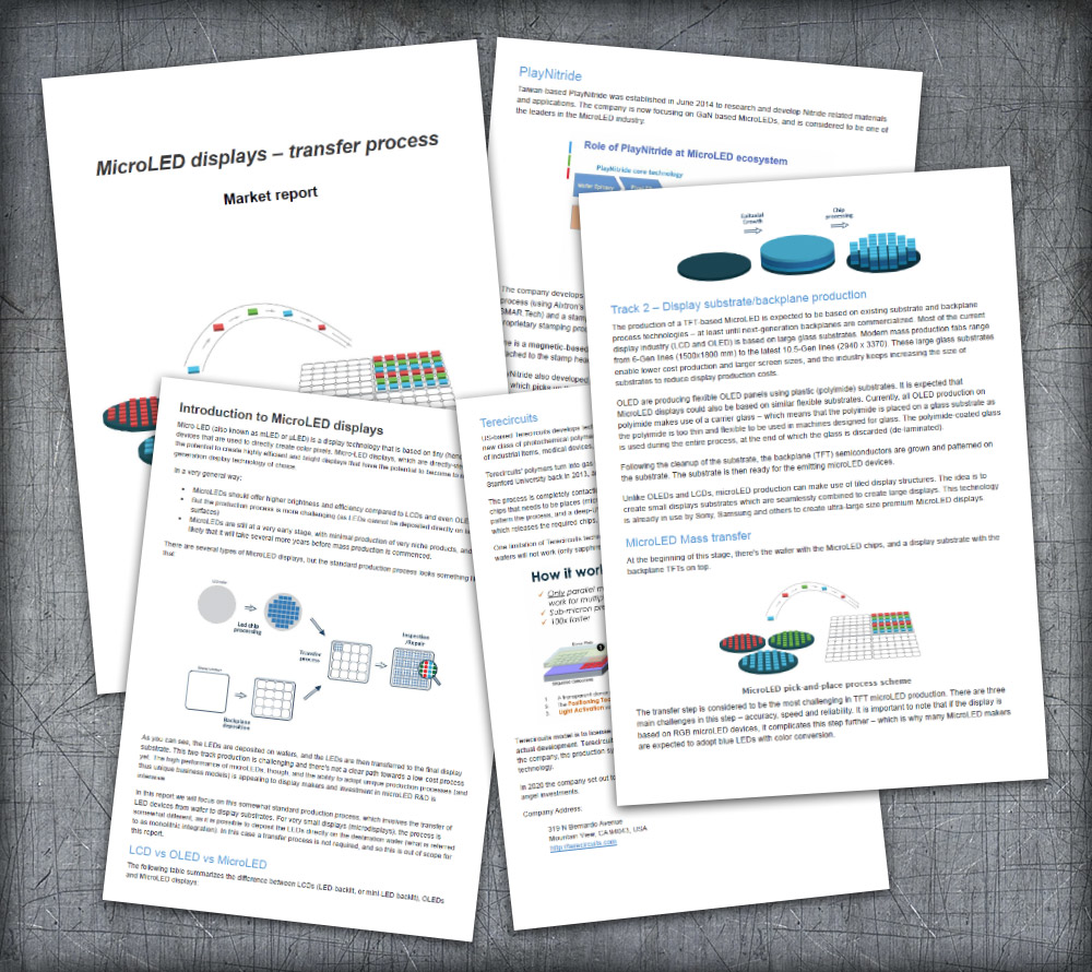
At the beginning of this stage, there's the wafer with the MicroLED chips, and a display substrate with the backplane TFTs on top. As we said, this is a challenging process, and there are three main challenges in this step – accuracy, speed and reliability.
It is important to note that if the display is based on RGB microLED devices, it complicates this step further – which is why many MicroLED makers are expected to adopt blue LEDs with color conversion.
Accuracy is an obvious issue – a microLED chip is extremely small and needs to be placed in the right place with very little room for errors.
Speed is another important consideration. Many displays today are of very high resolution – even smartphone displays are approaching 4K resolutions. A 4K display uses over 24 million subpixels. Even with mass transfer tools this is still a challenge as the display industry relies on quick and cost-effective production to achieve low costs.
Reliability is of course important. In the current LCD and OLED industries, producers manage to achieve extremely high yields and as display resolution and sizes increase, yields become more critical. The microLED yield issue will be discussed in a section below.
As can be expected for such a complicated process, several different technologies have been developed over the last few years. Most companies seem to focus on a stamp-based process. There are several ways to develop a stamp that can pick-up, hold, move and release microLEDs - using Van der Waals forces, using electrostatic charge, using magnetics, adhesives and more. Some companies look at novel ways to achieve the pick and place process - using fluidic assembly, or photochemical polymers. We will detail all public transfer process technologies below.
Some researchers classify transfer processes as follows:
- Stamp pick and place
- Self-assembly
- Selective release
- Roll printing
The transfer process needs to do more than just transfer the LEDs as-is. One issue is spacing (also called Pitch enlargement) – the microLEDs in the source wafer are packed together, close to each other – but on the final display they need to be spaced apart (the amount depends on the pixel pitch of the display). In addition, as we will detail below, defects in the epiwafer production phase (which will be very difficult to be rid of completely) mean that some LEDs will have to be skipped altogether.

The need for microLED spacing (source: eLux)
The basic transfer process moves the LEDs directly from the original wafer to the display substrate. Some processes, however, use an intermediate substrate (also called interposer). There could be several reasons why this is beneficial. For example, this could solve the problem of defective LEDs, could perform the spacing of LEDs and more.
Production yields, inspection and repair
Unlike the early days of LCD displays, consumers today will not accept even a single faulty pixel in a display (let alone a high-end new technology-based display). As production processes are never 100% free of faults, yield in display production is critical for efficient and satisfactory production.
In MicroLED display process, there are two main points where inspection is needed.
The first one is at the MicroLED production process – after the epiwafer stage and the chip processing stage, where it is vital to test the microLED chips for defects and quality.
The second major inspection stage is following the transfer process, which can also result in damaged chips. Following this step, it may be required to repair defective LEDs. Some microLED transfer technology developers integrate an inspection and repair process inside the transfer process, which seems to be an important advantage. Some industry experts say that yield loss could be the single biggest detriment for low cost MicroLED production.
A MicroLED display may include millions of individual LEDs. A 4K display has over 24 million subpixels, while an 8K display around 100 million. This means that at even very high yields, defective LEDs will not be avoided. At 99.99999% yields, there will be around 2 defective LEDs in each 4K display. This means that some repair solution will have to be implemented.
MicroLED production without transfer
As the pick and place process is extremely challenging, a microLED production process that will not require this step could be highly interesting.
One example is US-based iBeam Materials, which has developed an ion-beam based technology for crystal alignment of thin layers on a variety of large-area substrates, including thin, flexible large-area metal foils. Such a technology could be used to produce microLED devices directly on large-area flexible substrates. In September 2019, iBeam announced it has received an investment from Samsung Ventures to accelerate its microLED development. This technology is at a very early stage, but hopefully in the future it (or some other technology) could mature into commercialization.
MicroLED-Info's Transfer Process Report
This article was taken from our MicroLED Transfer Process Report, which expands on the transfer process, details over a dozen processes by leading companies, and contains over 20 presentations, patent descriptions and brochures by transfer process developers. You can order the report here.
Comments
Van der Waals - not 'van der
Van der Waals - not 'van der walls' :)
In reply to Van der Waals - not 'van der by Anonymous (not verified)
Yes, sorry for the typo, this
Yes, sorry for the typo, this was fixed!
Yes, sorry for the typo, this
Yes, sorry for the typo, this was fixed!
Van der Waals - not 'van der
Van der Waals - not 'van der walls' :)