STRATACACHE CEO details the challenges and goals of the company's upcoming US-based microLED display production fab

Global digital signage solution provider STRATACACHE is constructing the first US-based complete display production facility in Eugene, Oregon. The future MicroLED E4 fab is planned to commence production in 2022, and the fab will be a complete microLED production line, from epiwafer (on 300 mm silicon wafers), through transfer process and to final module assembly.

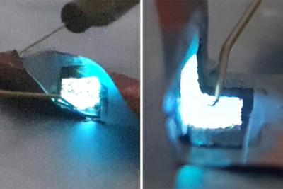
STRATACACHE Eugene E4 MicroLED fab photo

This project is extremely interesting, and we set out to discuss it with STRATACACHE's founder and CEO, Chris Riegel. At STRATACACHE, Chris leads strategic direction, technology development and engineering operations, and the MicroLED fab project seems to be personally spearheaded by him.

Read the full story Posted: Feb 27,2021

Coherent reports significant increase in MicroLED display system bookings, supplies laser systems to almost the entire industry

Laser equipment maker Coherent says that it saw a "significant increase" in the level of investment and bookings related to MicroLED displays. These tools are going to be used for process development, as a precursor to mass production.

Coherent reveals that its MicroLED customer base includes almost all current OLED and LCD manufacturers and many well-known MicroLED specific startups and display industry integrators. Coherent is offering multiple UV solutions for four separate MicroLED processes - CLA for high performance low power consumption back planes, laser lift-off for customers using sapphire carrier, laser transfer and laser repair.

Read the full story Posted: Nov 11,2020

Researchers use graphene to create detachable flexible microLED devices

Researchers from the University of Texas at Dallas developed a new method to create highly flexible microLED chips, that can be folded and twisted. The LEDs are detachable, and can be attached to almost an surface.

Flexible MicroLED devices, University of Texas (September 2020)

The researchers used remote epitaxy, to grow the LED crystals on a sapphire crystal substrate, coated with a one-atom layer of 2D graphene, which prevents the LED to stick to the sapphire substrate.

Read the full story Posted: Sep 01,2020

Sapphire nano-membranes enable higher-efficiency microLEDs

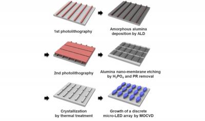
Researchers from Seoul National University (SNU) in collaboration with KAIST, SAIT and the Korea Photonics Institute developed a new method to deposit MicroLEDs on sapphire nano-membranes which enables chip singulation without an etching process. This method can enable higher efficiency MicroLED devices.

MicroLEDs grown on sapphire nano-membranes (SNU)

The researchers say that this method improves the internal quantum efficiency (IQE) of the microLEDs by 44% compared to standard GaN microLEDs produced on regular planar substrates. The microLEDs also featured a reduced dislocation density (by 59.6%). According to their tests, the microLEDs provided 3.3X the photoluminescence compared to regular microLEDs.

Read the full story Posted: May 11,2020

ALLOS and Veeco up-scale GaN-on-Si microLED production technology to 300 mm wafers

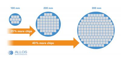
German-based GaN-on-Si developer ALLOS has applied its technology to large 300 mm epiwafers. ALLOS says that scaling up to 300 mm wafers enables higher production efficiencies and thus lower costs. ALLOS estimates that the higher area utilization alone accounts for a cost advantage of 40% compared to standard LED wafers. Standard 300 mm silicon line tools also offer higher production uniformity and yield.

Scaling up from 100 mm to 300 mm silicon wafers (ALLOS Semi)

ALLOS demonstrated the 300 mm scale-up using a reactor made by Veeco who announced selling the first 300 mm GaN reactor to a leading-edge semiconductor fab just some month ago and also showed 300 mm wafer data at CES. ALLOS reports a wavelength uniformity of consistently below 1 nm and "all other production requirements like bow of

Read the full story Posted: Apr 07,2020

Plessey developed a process to produce native GaN-on-Si green micro-LEDs

UK-based GaN-on-Si MicroLED developer Plessey Semiconductor developed its proprietary 2D planar gallium nitride on silicon (GaN-on-Si) process to emit Green light without the need for color conversion techniques.

Plessey native GaN-on-Si green micro LEDs photo

Plessey says that its native Green LEDs are formed inherently using its proprietary GaN-on-Si epitaxial growth process similar to the native Blue LEDs with the principal difference coming in the amount of indium that is incorporated in the quantum well structures of the LED. The native Green emission is orders of magnitude times brighter than color-converted process for micro-LEDs.

Read the full story Posted: Mar 29,2019

Optovate reveals its p-LLO micro-LED transfer process

UK-based Optovate recently announced that it has developed a parallel aligned Micro-LED transfer process. Today the company revealed more details about its Micro-LED technology.

Optovate p-LLO process photoOptovate p-LLO transfer process

Since 2008, Optovate develops catadioptric micro-optic arrays to enhance the benefits of micro-LED, mini-LED and OLED displays. The company also developed a patterned laser lift-off (p-LLO) micro-LED transfer process.

Read the full story Posted: Apr 25,2018