This is a guest post, by Ioannis (John) Kymissis
Micro light-emitting diode (microLED) technology is the bright young thing in the display world, literally and figuratively. Its high luminance, sharp contrast, and vivid colors, among other attributes, make this one of the most dynamic emerging technologies for next-gen display applications. We’re just beginning to see what the future holds for microLEDs and their potential impact on display and imaging capabilities.
On the Technology Fast Track
MicroLEDs have made rapid advancements since they were first submitted for patent in 1998. The Kansas State University researchers who developed these miniaturized versions of LEDs envisioned using them in sensors, detectors, and mini-displays. But now, in just under three decades, many major display leaders and emerging companies are racing to produce and integrate the technology in everything from smartwatches to TVs to automotive displays.
This industry-wide excitement is justified. MicroLEDs boast several specific characteristics that are advantageous for display, and for meeting the growing consumer demand for crisp, high-definition images that appear to be almost lifelike:
- Ultra-high brightness that’s greater than LCD and OLED, two of today’s most common display technologies
- Self-emissive properties that deliver picture quality with true black and high contrast ratios
- A wider color gamut with color conversion using quantum dots (QD) and phosphors
- Energy efficiency
- Durability and longevity, with less susceptibility to burn-in than OLED
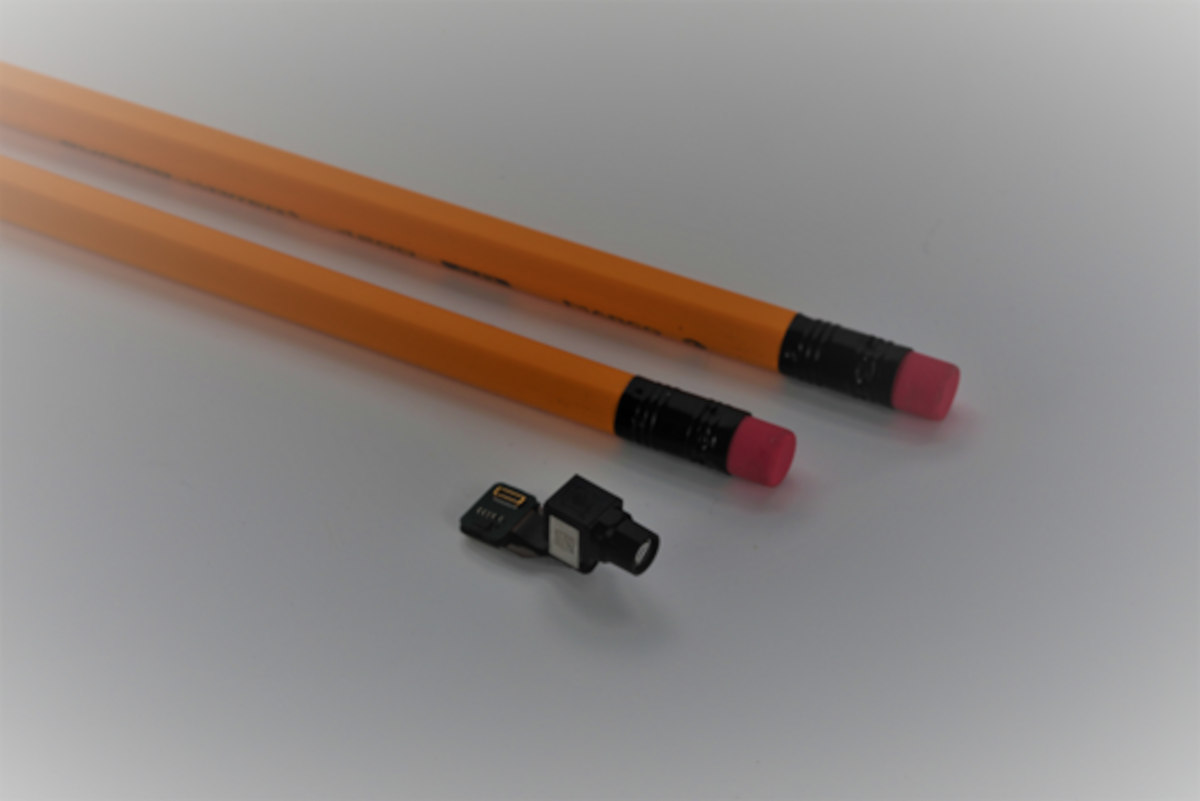
The microLED evolution is underway, but the pace of change is dictated by scalability, and there are some challenges to work through. Manufacturing microLEDs is a complex process (and it gets even more complex if QD and phosphor integration are added to the mix). Assembling microLED driving backplanes (the electronic circuitry powering this technology) involves millions of pixels, and the two most common approaches for industrial-scale manufacturing — mass transfer technology and monolithic integration technique — each have their pluses and minuses. Finally, production and processing costs are still expensive, which can be a roadblock for mass-market microLED applications.
MicroLEDS in Action
Even with these challenges, however, the field of microLED applications is ripe with innovative ideas. The products and prototypes we’re seeing are impressive, and not just in display technology; microLEDs are being implemented in non-display applications as transmitters in visible light communication, while optical sectioning microscopy systems use the technology for backlighting and pattern generation.
Currently, microLEDs are making a significant impact in two main areas of display and imaging. AR/VR applications using microLEDs are compact and lightweight because the display doesn’t require a backlight to be seen, which is helpful for wearables like smart goggles or glasses. These devices can also be used outdoors because the microLED system requires little power to operate and offers enough brightness for the display to be seen in daylight. And the contrast and color quality provide the type of hyper-realistic images that are most desirable in AR/VR.
MicroLEDs are also poised to transform small form factor display applications, like cell phones and smartwatches. With monolithic integration, microLEDs can be produced with exceptional pixel-per-inch (PPI) density in these microdisplays. This high visual quality is enhanced by microLEDs’ superior luminance, giving these applications the much-needed versatility to be used indoors and outdoors. Because microformats reduce manufacturing challenges and costs, these direct-view microLED applications are likely the first that will be adopted by consumers on a large scale.
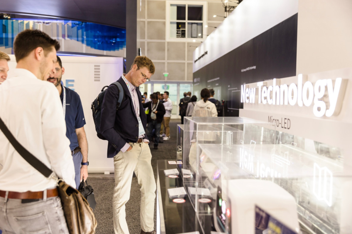
There’s so much potential to explore because we’re discovering new ways to utilize the creative freedom offered by microLEDs. The best place to see these groundbreaking ideas come to life is at Display Week. Presented by the Society for Information Display (SID), this is the world’s largest technical symposium and exhibition. It’s also a showcase for SID’s Display Industry Awards (DIA) winners, representing the best-in-class display and imaging products and technologies. Several recent DIA winners include microLED products, such as:
- Jade Bird Display’s 0.13-inch Active Matrix MicroLED Microdisplay (which is already in use in several AR applications such as smart glasses, sports goggles, and heads-up displays for motorcycles)
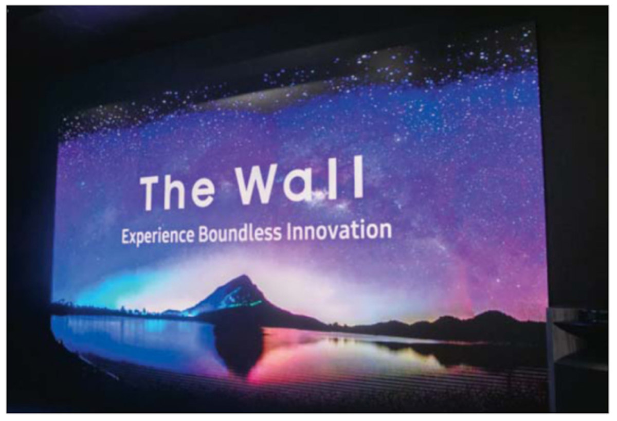
- Samsung’s Modular MicroLED Display (also known as The Wall, this award winner facilitates customized or unique display formats)
- Sony’s Crystal LED Displays (immersive, borderless panels can be tiled to create seamless, immersive display images on a large scale)
Will MicroLED Be in the DIA Winner’s Circle in 2024?
Plenty of microLED innovation will be on the exhibition floor at Display Week this year, from potential DIA honorees to new-to-market products in the I-Zone. Attendees from more than 50 countries and almost every industry sector come to Display Week because they want to be the first to see the latest microLED advancements, including transparent and non-flat applications, wearable displays, and upgrades in the electronics that control LED systems.
Display Week’s technical programming will also focus on important areas relevant to microLEDs. Sessions include in-depth discussions of digital and e-signage displays, active-matrix devices, AR/VR/MR, automotive displays, display-module manufacturing, and much more. There is also a symposium segment devoted to emissive, microLED, and quantum dot (QD) based technology topics - follow the EMQ subcommittee at Display Week for these topics.
Display Week 2024 takes place May 12-17 in San Jose, California. Be there and witness firsthand the bright future ahead for microLED technology.

Ioannis (John) Kymissis is the Kenneth Brayer Professor of Electrical Engineering at Columbia University. He graduated with his SB, M.Eng., and Ph.D. degrees from MIT. His M.Eng. thesis was performed as a co-op at the IBM TJ Watson Research Lab on organic thin-film transistors, and his Ph.D. was obtained in the Microsystems Technology Lab at MIT, working on field-emission displays. After a post-doc and work at QDVision, he joined the faculty at Columbia University in electrical engineering in 2006 as an assistant professor, and is currently serving as chair of the department. Kymissis has won a number of awards for his work, including the NSF CAREER award, the IEEE EDS Paul Rappaport award, and the MIT Clean Energy Prize. He is a fellow of SID, IEEE, and Optical, and is the President-Elect of SID.