This is a sponsored post by Radiant Vision Systems
Introduction
MicroLEDs (micro-LEDs, mLEDs, or μLEDs) continue to demonstrate performance advantages for displays, ushering in a new generation of backlit and direct-view illumination technology. MicroLED displays consist of an array of microscopic LEDs (light emitting diodes) that form the display’s individual subpixel elements. This inorganic emissive technology offers many benefits over rival display technologies, including higher brightness and contrast, wider color gamut, and higher pixel density. MicroLEDs enable improved visual performance in ambient-light conditions, from total darkness to full daylight and when viewed from multiple viewing angles. These qualities make microLEDs especially attractive for applications such as mobile phones and watches, augmented- and mixed-reality (AR/MR) headsets, automotive display panels, and digital signage.
Challenges associated with manufacturing high-quality microLED panels continue to hinder production efficiency and must be addressed before manufacturers can achieve commercially viable microLED display products. Producing displays with the level of visual quality customers expect while keeping component and production costs low demands quality control solutions that reduce waste while increasing yield of acceptable displays.
The Challenge of MicroLED Display Uniformity
Achieving a consistent, uniform appearance has been a significant challenge in microLED component production. As individual emissive elements, microLEDs are driven independently and can exhibit a high degree of variability in luminance and color (see Figures 1 and 2). This variability can render microLED components unusable unless corrections are applied to improve uniformity across each emissive element and at all bright states.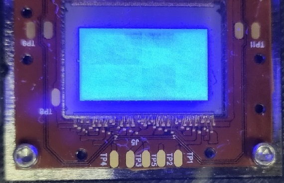
Figure 1. This close-up image of a microLED microdisplay panel demonstrates the potential luminance and color uniformity issues resulting from varying microLED pixel output across the display.
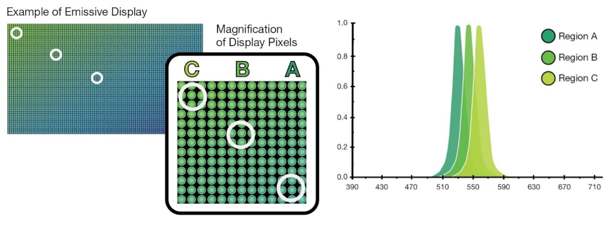
Figure 2. Illustration of an emissive display with color variability (far left), with magnification of display pixels A, B, and C at different points on the display (center left); example of varying spectral data for A, B, and C (right).
Variability in a display is compounded because each microLED is a monochromatic subpixel (typically red, green, or blue) whose output is combined with other subpixels to produce the overall brightness and color of a single display pixel. This variability at the subpixel and pixel level manifests as a non-uniform appearance across the display, resulting in low yield of acceptable displays, rejection of expensive components, or costly rework (Figure 3).
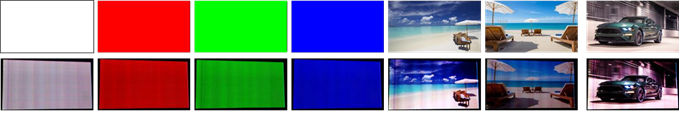
Figure 3. Input signals for target color gamut of DCP-P3 (D65) (row 1), compared to actual microLED display output (row 2), where a dominant vertical pattern and block-wise stamp marks are clearly seen.1 (Images © Samsung Research / Samsung Electronics)
Measurement of microLED subpixels is necessary to sufficiently quantify, evaluate, and correct display pixel output. However, microLEDs are challenging to measure with high accuracy due to their variable luminance and color, as well as their size, proximity, and quantity per display. This makes them equally challenging to correct—especially at the speed needed to support commercial production throughput demands.
Correcting Emissive Displays
Display manufacturers have long used correction methods (electronic compensation, or calibration) to improve visual quality. The concept is simple: by modifying the inputs to individual subpixels of an emissive display, previously identified dim pixels can be adjusted to a uniform luminance level at each bright state, resulting in uniform brightness and color appearance across the display at all states.
Display correction requires, first, having in-display electronics that can control inputs to the individual subpixels and make adjustments based on the calculated correction factors for each subpixel. Second, a measurement system is required to accurately quantify individual subpixel luminance and chromaticity values, and compute specific correction factors for each subpixel at each bright state. This method was originally developed to calibrate LED video screens and has been adapted for today’s high-resolution emissive displays (OLED and microLED) using a correction technique known as “demura†or pixel uniformity correction (PUC).
Demura. The demura method employs three distinct steps:
- Measure each subpixel in the display to calculate luminance values at each pixel coordinate location using a high-resolution imaging colorimeter. Test images are driven to the display to target subpixels of each color set. These images enable measurements and correction factors to be computed for each set. For example, a green test image can be driven to the display to illuminate all green subpixels. An imaging colorimeter measures and records the output of each green subpixel. This is repeated for all primaries (red, green, blue) and, usually, white.
- Load measurement data from each display pixel’s coordinate position into a coefficient calculator. Correction factors are calculated to normalize luminance and chromaticity discrepancies between pixels in the display using test analysis software.
- Apply correction factors to the signals of each subpixel at each pixel location using an external control IC (integrated circuit) system.
A measurement and correction system applied in microLED manufacture must be capable of precise quantification of each subpixel with very low takt times to correct the high quantity of emitters in a single display at production speeds. Test and measurement solutions are evolving to address microLED display quality, combining traditional automated visual inspection systems with innovative methods to improve accuracy while maintaining efficiency.
Considerations for MicroLED Measurement
Different display metrology systems offer unique benefits and drawbacks when applied for microLED subpixel measurement. For example, a spectroradiometric system can achieve a high degree of measurement accuracy (both luminance and chromaticity), but slow takt times make it an inefficient solution to measure the millions of pixels that make up an entire microLED display.
Additionally, spectroradiometric systems typically have a spot size that is too large to provide the most accurate measurement of individual microLED emitters. A typical microLED is 2 (see Figure 4). A measurement system such as a spectroradiometer capable of measuring structures with a diameter down to 0.075 mm would be insufficient to differentiate and measure the characteristics of individual microLEDs typically smaller than 75 μm.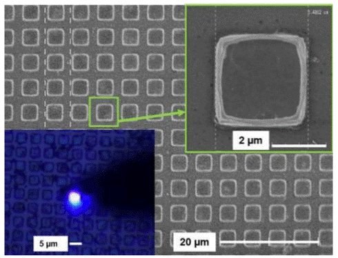
Figure 4. SEM micrograph of 3-μm size / 5-μm pitch microLED array. Inset lower left is an optical photograph of a microLED powered on. (Image © Leti)
To meet production takt time requirements, high-speed machine vision cameras are sometimes employed for automated visual display inspection. However, these systems do not innately provide photometric and colorimetric accuracy required to quantify differences in luminance and chromaticity values, especially at the subpixel level.
As will be shown, a calibrated, high-resolution imaging colorimeter provides both the accuracy and speed to meet production needs, and thus offers an effective solution for pixel- and subpixel-level measurement of microLEDs in production. An optimal measurement solution for addressing commercial manufacturing demands would include:
- Imaging colorimeter. The advantages of imaging colorimeter and photometer systems include efficiency—the ability to detect all meaningful variations across displays in a single image, accomplishing multiple measurements at once: luminance, chromaticity, uniformity, contrast, pixel defects, etc. Another advantage is scope—the ability to capture the entire field of view (FOV) of a display in a single image, just as the device is viewed by a user. An imaging photometer measures luminance, while an imaging colorimeter measures luminance and chromaticity.
- High resolution. A microLED measurement system must have high-resolution imaging capabilities. High-resolution imaging provides the precision needed to distinguish and isolate each pixel and subpixel for measurement, and the efficiency to capture values for every pixel across increasingly high-resolution and pixel-dense displays in a single image.
- Low noise. Low-noise imaging capability is also needed. Image noise (which can include read noise, shot noise, or electronic noise) interferes with the clarity of an image. No matter how high the resolution of an imaging system (the number of megapixels (MP) of its sensor), if the system captures significant noise per sensor pixel (yielding low signal-to-noise ratio, or SNR), then the system’s effective resolution may be much lower.
- Calibration. To perform accurate measurement according to CIE standards, a metrology device must be carefully calibrated. A common method uses reference data captured by a spectrometer to calibrate the response of an imaging colorimeter. Enhanced Color Calibrationâ„¢ (ECC) is an algorithm-based calibration method shown to improve accuracy for highly variable sources (see the Enhanced Color Calibration section below).
- Test & Analysis Tools. Image processing software enables manufacturers to optimize and run tests on a captured image. Ideally, an analysis package for display measurement would include tools to detect and quantify luminance, chromaticity, uniformity, contrast, pixel & line defects, display mura, and other qualities. Algorithms to optimize imaging precision for subpixel registration and measurement are additional beneficial features that increase display test efficiency when included in out-of-the-box solutions.
The Importance of Measurement Accuracy: Luminance and Chromaticity
In 1931, the Commission Internationale de L’éclairage (CIE) defined a standard for scientifically quantifying the physical properties of color as perceived by a human observer, enabling accurate mathematical representation and reproduction of those colors (Figure 5). 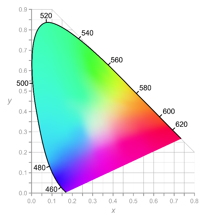 Figure 5. A graphical representation of the CIE 1931 color space, including all colors visible to the human eye. The black numbers on the edge give the visible spectrum in wavelengths, while perceived colors are represented as coordinate points (x and y) within these limits.
To ensure accuracy when measuring highly variable microLEDs, a measurement system is needed that can discern color variation with equivalent sensitivity to the human eye. A standard human spectral sensitivity is quantified through mathematical formula of the CIE standard to provide chromaticity values as coordinates within the CIE color space.3
Tristimulus (XYZ) color filters on a rotating filter wheel enable imaging systems to perform color measurement according to standard CIE color-matching functions and chromaticity values. Light entering the metrology device is passed through the respective filters and then captured by a sensor (see Figure 6). The filters adjust the incoming light, blocking certain wavelengths (such as UV that are invisible to the human eye) so that the sensor captures a measurement image with values that are as close as possible to what the human eye perceives.
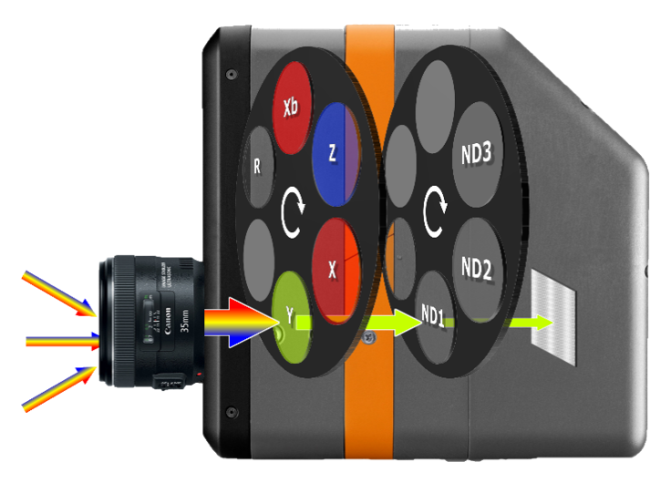
Figure 6. A CIE-matched tristimulus filter wheel system (shown here inside a ProMetric® I-series Imaging Colorimeter from Radiant Vision Systems) enables a measurement device to capture light and color as values that reflect the spectral sensitivity of the human eye.
Tristimulus Systems. A recent study by Jensen, Piehl, and Renner (2020)4 demonstrates the high degree of accuracy of a tristimulus filter wheel system for CIE standard color measurement (for details, see the section below titled Measurement Accuracy Study: Tristimulus System).
Enhanced Color Calibrationâ„¢. All imaging systems used for metrology applications require calibration data from a spectrometer or other device to ensure measurement accuracy. Enhanced Color Calibration (ECC) from Radiant Vision Systems provides the highest level of color measurement accuracy using advanced calibration algorithms. The ECC method creates a 12-element correction calibration matrix to maximize the ability of the color measurement system to tolerate variability (provide accurate color measurement over a large area of the CIE color space) from a calibrated color value (calibration point; see Figure 7).
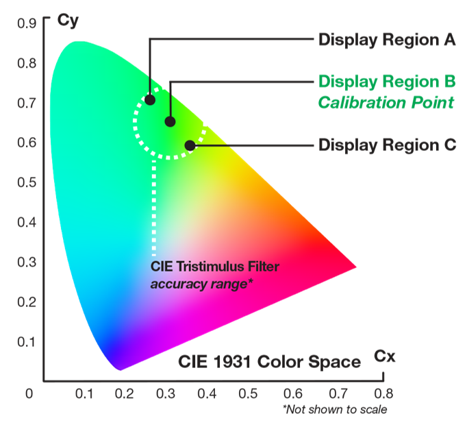
Figure 7. ECC enables a tristimulus imaging colorimeter to continue to provide accuracy even as source spectral data deviates further from the calibration point. This chart illustrates an expected accuracy limit (area within the white dotted line circle) for a tristimulus imaging colorimeter for measuring display pixels A, B, and C plotted from Figure 2.
Measurement Accuracy Study: Tristimulus System
The study below evaluates the color measurement accuracy of a tristimulus-filter-based imaging colorimeter system using ECC (Radiant Vision Systems ProMetric® I29 (29MP) Imaging Colorimeter) compared to a reference meter (a spectroradiometer). LEDs of different colors were measured by the reference meter and by the imaging colorimeter.
First, the imaging colorimeter was calibrated to a base output for each LED (using ECC). Then, each system measured each LED as its output was varied (LED variability was introduced by supplying different current levels). The accuracy of the imaging colorimeter was defined by its ability to match reference meter measurements as chromatic distance of the LED output increased from the system calibration point.
Results. The measurement data plotted in Figures 8 and 9 demonstrate that a tristimulus system provides accurate luminance and chromaticity values across introduced LED source variation. The tristimulus system measurements vary from reference meter measurements by less than 0.0050 Δxy (CIE 1931) for nearly all LEDs. In this study, the introduced variability of the LED test sources exceeded the expected variability of microLED sources. These results demonstrate that a tristimulus system with ECC can measure LEDs with a high degree of accuracy in both luminance and chromaticity—even as sources vary widely from the calibration point. A tristimulus system is recommended for ensuring efficient and accurate display measurement and correction where pixel output variation is high, or tolerance for variation is limited.
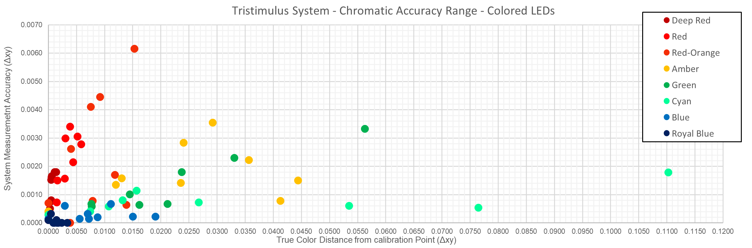
Figure 8. Tristimulus system (ProMetric I29 Imaging Colorimeter) accuracy range for color variation across colored LED test sources.
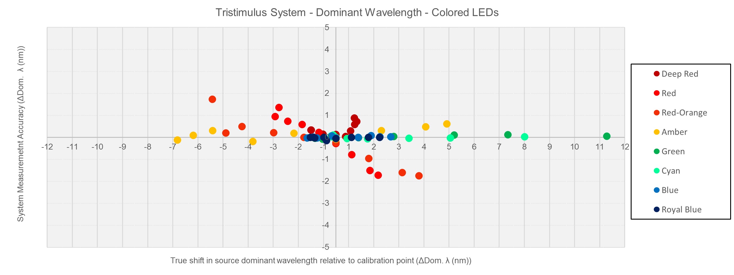
Figure 9. Plot showing true LED source variation at each current level (as measured by the reference spectroradiometer) based on ± nm change in dominant wavelength from the calibration point (x-axis). This axis gives the range of variation observed for each LED. The tristimulus system (ProMetric I29) measurement accuracy is shown as a ± nm difference from the reference measurement at each current level for each LED source (y-axis).
The Importance of Measurement Accuracy: Pixel-Level Resolution
As noted previously, microLED size ranges from less than 100 μm to as small as 3 μm—about 1/10th the width of a human hair.2 Measurement accuracy within the small area of an individual microLED depends on imaging resolution and signal processing methods. To increase yields through display correction, it is essential to be able to isolate and measure each individual microLED emitter with precision so luminance or chromaticity values specific to a given microLED can be corrected. A high-resolution imaging system optimizes the number of photo-sensing elements (sensor pixels) applied across each microLED for accurate subpixel measurements and offers sufficient resolution to ensure all microLEDs in the display can be measured at once to complete correction processes within adequate takt times. Measurement systems that use tristimulus filter wheels further maximize resolution by combining multiple images (one for each color channel) for a single measurement, each image at full-sensor resolution (see Figure 6, above).
Beyond display uniformity requirements, general visual performance standards in the display industry allow for less than 10 dead pixels per display, which can occur at any point in microLED production. Ensuring microLED display quality demands precise measurement at the LED, chip, wafer, and panel stage to reduce the possibility of dead pixels and evaluate uniformity before defects are introduced to subsequent stages.
LED, Chip, and Wafer-Level Measurement. For inspection of individual microLEDs, chips, and wafers, a high-resolution, low-noise imaging colorimeter with a standard lens or microscope objective lens can be used. A microscope lens provides measurement with, for example, 5X or 10X zoom (5 to 10 times the effective resolution of the imaging system applied over an area of the LED or component), allowing detailed measurement of each individual emissive element (see Figure 10). Used with a high-resolution imaging system, a microscope lens enables every display subpixel or LED to be captured over several image sensor pixels for increased measurement precision.
Panel-Level Measurement. Once individual microLED chips are transferred onto a backplane, an imaging colorimeter with standard lens can be used to measure subpixel luminance and chromaticity values across the entire panel at once. The advantage of an imaging colorimeter is its ability to capture a large area in a single image to evaluate uniformity quickly and accurately, just as a user would view a display.
High-resolution imaging systems must continue to provide pixel- and subpixel-level measurement accuracy to ensure appropriate uniformity correction, even as the number of pixels per display panel increase. Higher-resolution displays increase the demand on even the highest-resolution imaging systems. Capitalizing on the efficiency of single-image display measurement reduces the number of image sensor pixels that can be applied to measure each display pixel, which may reduce the accuracy of pixel- and subpixel-level measurement data if advanced imaging and signal processing methods are not applied.
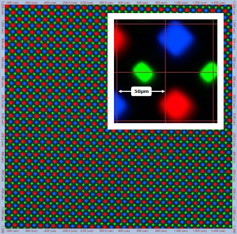
Figure 10. Example of subpixel measurement (main image) taken by a ProMetric I29 Imaging Colorimeter and a Radiant Microscope Lens, magnified to show 50 μm distance at 10X zoom (inset image).
Figure 11. Microscope Lens and ProMetric imaging system from Radiant Vision Systems.
Methods to Improve Pixel Registration and Measurement
Accurate subpixel-level measurement relies on a measurement system’s ability to sufficiently isolate each display pixel and precisely quantify its output value. As described above, imaging resolution determines the number of photo-sensing elements (sensor pixels) available to cover each individual display pixel. Applying more sensor pixels per display pixel increases the granularity of data acquired by the imaging system for accurate pixel registration and pixel measurement. As overall display resolution increases, an imaging system’s ability to apply sufficient sensor pixels per display pixel—while continuing to capture measurements for all display pixels on a panel in a single image to ensure efficiency—is reduced.
Two methods developed by Radiant Vision Systems have been proven to significantly improve an imaging system’s ability to isolate and measure subpixels of increasingly high-resolution displays for correction: a “spaced pixel†method and a “fractional pixel†method; both are described below.
Spaced Pixel Method. The spaced pixel measurement method (US Patent 9135851) improves the effective resolution of a measurement by applying the measurement system’s total image sensor resolution across only a subset of display pixels at a time. The method employs a series of dot-matrix test patterns shown on the display screen as part of a measurement sequence. Each pattern illuminates a subset of the display’s pixels, while the rest are turned off. An imaging colorimeter measures the output (luminance or chromaticity) of the “on†pixels for each pattern. A subsequent test image adjusts the matrix to turn off the first set of pixels and turn on the next set of pixels for measurement. This process is repeated until all pixels in the display are measured.
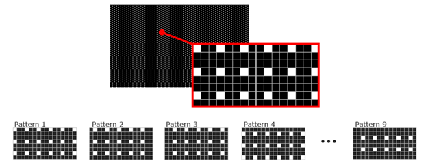
Figure 12. During spaced pixel measurement, a series of dot-matrix patterns illuminates sets of pixels until values have been acquired for all pixels in the display.
This process increases the effective resolution of the measurement at each display pixel, ensuring the isolation of each pixel’s output, and thus the accuracy of measurement calculations across displays of any arbitrary resolution. Images from the spaced pixel measurement method are combined into a single, synthetic image for analysis, which compares values at each of the pixel’s x,y coordinate locations to determine uniformity. Software calculates the necessary correction coefficient for each display pixel and applies the correction at each pixel’s coordinate location to adjust values until the display is uniform.
The spaced pixel method reduces the requirement for measurement resolution to increase measurement accuracy. However, because this method requires multiple images, takt times are also increased. The fractional pixel method (explained in the next section), by comparison, improves measurement accuracy without increasing takt times—for example, only a single measurement image is required to evaluate all pixels in a typical smartphone display. Thus, the fractional pixel method offers advantages when shorter takt times are required, as in many production-level test and correction applications.
Fractional Pixel Method. The fractional pixel method addresses measurement scenarios where imaging sensor resolution per display pixel is limited, enabling measurement systems with standard resolutions to continue to accurately measure and correct today’s high-resolution displays, even in a single-image measurement of the entire display.
First, the fractional pixel method optimizes pixel registration. Pixel registration is a method of dynamically locating and setting a region of interest (ROI) around each pixel in the measurement image. In traditional methods, ROI are aligned to the imaging system’s sensor pixel array. However, as display resolutions continue to increase relative to measurement system resolutions, it is more likely that the center of a display pixel will not be aligned with the center of a sensor pixel, reducing the ability of the ROI to precisely cover and isolate each display pixel. This misalignment can result in measurement error. By comparison, the fractional pixel method sets a registration area around each display pixel using a floating point, aligning the ROI to the center of a display pixel based on the highest measured luminance across the display pixel.
Second, the fractional pixel method optimizes pixel measurement. The fractional pixel method calculates display pixel output values based on the fractional area of each sensor pixel contained within the ROI (see Figure 13, right image). This improves the precision of measured values over traditional “whole pixel†methods that factor values from the whole area of sensor pixels contained only partially withing the ROI (see Figure 13, left image). The fractional pixel method ensures the accuracy of pixel-level measurements for extremely high-resolution emissive displays beyond what was previously possible using a single-image capture. With the fractional pixel method, imaging systems with limited resolution (relative to display resolution) can continue to measure pixel-level values across a display in a single image effectively, increasing takt time without reducing measurement accuracy.
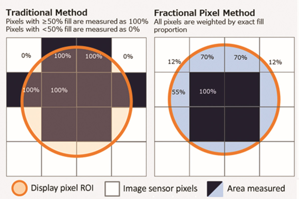
Figure 13. Illustration of a traditional whole pixel measurement method versus the fractional pixel method. In the traditional method (left), display pixels are measured using 100% of the data from sensor pixels whose area is more than 50% inside the ROI, and 0% of the data from sensor pixels whose area is less than 50% inside the ROI. Using the fractional pixel method (right), display pixels are measured using a percentage of data based on the percentage of sensor pixel area inside the ROI.
Measurement Accuracy Study: The Fractional Pixel Method
The accuracy of the fractional pixel method was demonstrated in a study published by Pedeville, Rouse, and Kreysar (2020).5 Figure 14 plots single-image measurement data from this study, comparing the pixel-level measurement accuracy of fractional pixel measurements, whole pixel measurements, and extremely high-resolution reference measurements. The fractional pixel data adheres closely to the reference data, whereas the whole pixel measurements diverge from the reference data at multiple points.
Figure 15 shows the before-and-after result of an actual measurement and correction (demura) application applied by Radiant Vision Systems using a 29MP ProMetric Imaging Photometer and both spaced and fractional pixel methods to correct a microLED microdisplay panel.
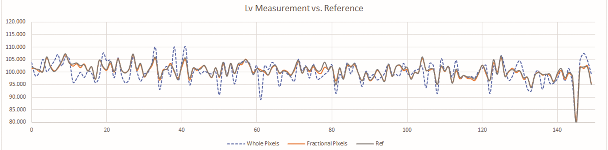
Figure 14. Normalized luminance (Lv) measured by whole and fractional pixel measurement methods (achieving 3.2 x 3.2 sensor pixels per display pixel) and reference luminance (achieving 30 x 30 sensor pixels per display pixel) for the same row of pixels on an emissive display.
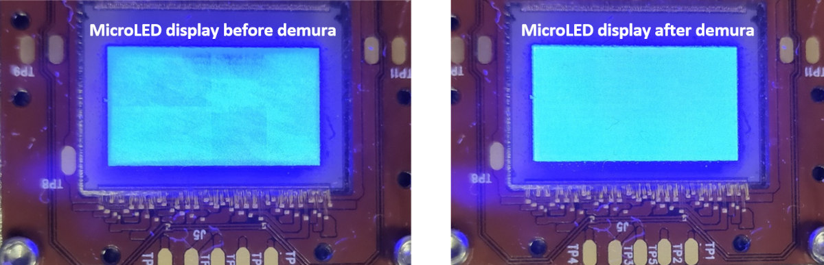
Figure 15. MicroLED microdisplay panel shown before (left) and after (right) demura correction. The panel shown is 0.7†with full HD, 1920 x 1080, and LED size/pitch of 2 μm/8 μm. Measurement and correction were performed using a ProMetric Y29 Imaging Photometer with Microscope Lens and TrueTestâ„¢ Software.
Conclusion
MicroLEDs are quickly taking their place in the highly competitive display marketplace. Developers are racing to find production solutions that deliver performance and exceed customer expectations, while maintaining cost-effective production processes and high yields.
Defects, variations in color or brightness, and other irregularities can quickly deflate buyer satisfaction, hurt brand reputation, and erode market share. If these issues cannot be addressed and corrected at the component level, low yields and high production costs will impede the viability of microLED display technologies for mass production and market commercialization.
High-resolution tristimulus imaging colorimeter systems provide an efficient solution to support quality and efficiency benchmarks for microLED production. These systems rely on their color filter method, calibrations, and subpixel measurement capabilities to ensure accurate data is captured at the pixel and subpixel level, enabling correction that safeguards manufacturing resources.
Studies of recent display metrology systems and measurement methods demonstrate the effectiveness of high-resolution tristimulus imaging systems, combined with sophisticated algorithms for calibration, registration, and measurement to solve microLED display uniformity challenges and support the viability of microLED technology for the display device marketplace.
Using imaging colorimeters and novel imaging methods, manufacturers at all stages of microLED manufacture (from LED to wafer to panel) can realize a solution for production efficiency that enables them to ensure quality, reduce waste, and continue to innovate high-performance displays in a range of types, sizes, and applications.
References
1. Kim, K., Lim, T., Kim, C., Park, S., Park, C., et al., “High precision color uniformity based on 4D transformation for micro-LED.†Proceedings of SPIE Vol. 11302, February 2020.
2. Lapedus, M., “MicroLEDs: The Next Revolution in Displays?†Semiconductor Engineering, May 2019. (Retrieved from https://semiengineering.com/microleds-the-next-revolution-in-displays/)
3. Carter, E., Schanda, J., Hirschler, R., Jost, S., Luo, M., Melgosa, M., … Wold, J., CIE 015:2018 Colorimetry, 4th Edition, 2018. DOI: 10.25039/tr.015.2018
4. Jensen, J., Piehl, A., and Renner, W., “Evaluating tristimulus and Bayer pattern matching system accuracy for color measurement based on CIE color-matching functions,†presented at the 34th annual electronic displays conference (edC), January 2020.
5. Pedeville, G., Rouse, J., and Kreysar, D., “Fractional Pixel Method for Improved Pixel-Level Measurement and Correction (Demura) of High-Resolution Displays,†Society for Information Display (SID) Display Week 2020 Digest, Book 2, August 2020.

