September 2022

LG launches a new 136" 4K microLED MAGNIT TV in the US

LG Electronics launched a new microLED TV in the US, the LG MAGNIT 4K 136-inch 2000-nits 120Hz Micro LED residential display (LSAD Series). This residential TV is a "luxury residential display' that is powered by LG's latest Alpha 9 AI-enhanced processor and the company's own webOS smart TV platform.

LG says that the new MicroLED display is available in the US through specially-certified LG distribution partners.

Read the full story Posted: Sep 30,2022

The MicroLED Industry Association to host a microLED technology webinar with UCSB professors DerBaars and Nakamura

On October 25th the MicroLED Industry Association will host a webinar on microLED technologies with the University of California, Santa Barbara. UCSB has a world-leading LED research program, led by Mitsubishi Distinguished Professor Steven DerBaars and Nobel Prize in Physics laureate Professor Shuji Nakamura, professor of materials and of electrical and computer engineering.

During the webinar, Prof. Nakamura and Prof. DenBaars will both give a lecture to update on the latest microLED research done at UCSB, and a few members of the MicroLED Association will also give a lecture to introduce their company technologies. There will also be time for questions, and an open discussion.

Read the full story Posted: Sep 28,2022

Focally unveils prototype AR glasses that use a full-color microLED display engine

India-based startup Focally unveils prototype AR glasses that feature several innovative technologies, including a full-color microLED based display engine.

Focally says that its Universe AR glasses will enable full-color and monochrome display modes, which leads us to believe that this display engine is built from 3 separate monochrome microLED displays, perhaps a similar design to Vuzix's display engine. Using waveguide optics, the company says that the display provides a 30-degree FOV. The company says that the display engine is the world's smallest and brightest, but does not provide any technical details.

Read the full story Posted: Sep 28,2022

C SEED announces new premium foldable outdoor microLED TV, the HLR series

In 2021, Austria-based C SEED released a high-end microLED TV, the $400,000 165" 4K C SEED M1, which has a unique foldable design, which makes use of seven large MicroLED panels.

C SEED now announced a new outdoor foldable MicroLED TV, called the HLR series. The displays (both based on seven panesl) offer a brightness of 4,000 nits and a resolution of 4K. There are two models, a 144" one which costs $298,000 and a 201" one that costs $590,000.

Read the full story Posted: Sep 28,2022

PlayNitride is working with customers on automotive microLED displays, expects first concept car demonstrations in 2024

Digitimes reports that PlayNitride is starting to sample microLED panels for 5 or 6 potential automotive customers. The customers are interested in flexible and transparent panels, and they have engaged PlayNitride in custom R&D projects to develop the required displays.

PlayNitride 9.38'''' transparent microLED prototype (Touch Taiwan 2022)

PlayNitride's CEO, Charles Li, noted that the company expects its customers to launch several concept car models in early 2024, equipped with the new microLED displays.

Read the full story Posted: Sep 27,2022

A new version of our MicroLED Transfer Process Market Report released

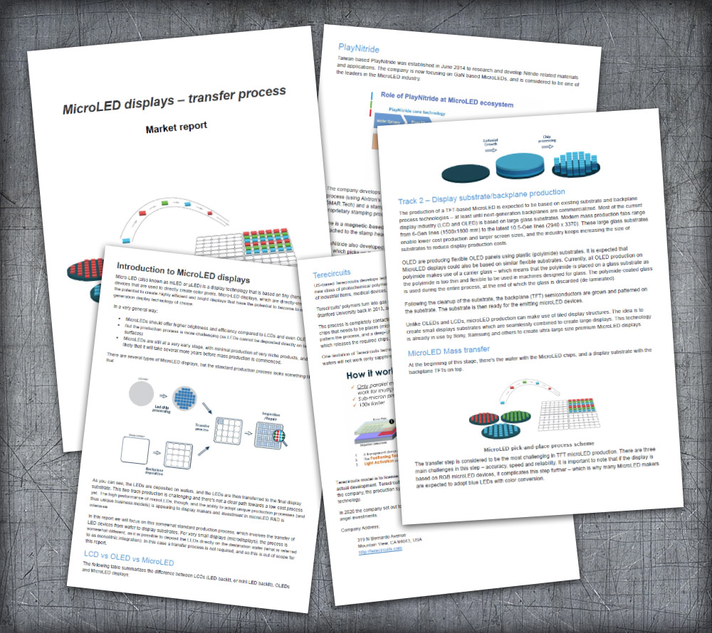
Today we published a new edition of our MicroLED Transfer Process Market Report, with all the latest information. The new edition includes news from related companies, new in-depth details on two transfer processes and more.

Reading this report, you'll learn all about:

  • All known microLED transfer processes
  • The current industry and market status
  • Advantages and disadvantages of transfer technologies
  • Future technologies and roadmaps

The report package also provides:

  • An introduction to microLED production processes
  • Over 20 presentations, brochures and technical papers
  • MicroLED chip-level market estimates and forecasts
  • Free updates for a year

This microLED display transfer process report provides a comprehensive look into current and future LED transfer technologies processes used for the production of microLED displays. The report covers everything you need to know about the current status of the industry.

Read the full story Posted: Sep 22,2022

MicroLED and QDs: Selected Technology Highlights by TechBlick

This is an article by TechBlick, organizers of the upcoming MicroLED Displays virtual event. MicroLED-Info readers get a 100 Euro discount.

In this article, using select technology slides, we highlight several interesting advancements in MicroLED and/or QD displays. More specifically, we cover 3600PPI “Silicon” Displays | Gravure printed microbumps | Electrohydrodynamically printed QD color converters | Laser LLO and Transfer for MicroLEDs | QD vs Phosphors | Energy saving credentials of microLED

“Silicon” Displays with an incredible 3600ppi full color using microLED and QD technology?

Sharp (HIRANO Yasuakie et al) has developed this technology.

As shown in the slide below, first blue-only uLEDs are formed on a sapphire substrate. Here, one LED array contains 352 x 198 micro LED dies of 24 um x 8 um in size. In parallel, an LSI chip containing the driving circuitry is formed on a silicon wafer. Here, the cathode (N-type electrode) and anode (P-type electrode) are fabricated for each micro LED die to apply driving voltage independently to each die. The Au bump electrodes are fabricated in accordance with the pitch of the LED dies. The two substrates are flip-chip bonded using Au-Au bonding. Here one can already see the parallel to the silicon and optoelectronic industry (vs. the traditional thin film display industry!). Next, the sapphire layer is removed via laser lift off. Finally, Cd-free quantum dots (green and red) are deposited atop the microLED dies to enable R G color conversion. This way one achieves RGB colors

The device architecture is shown in slide 2- here one can see the location of GaN uLED dies, Au bumps, as well as light shielding walls and quantum dots (QDs). This way, a full color 1,053 ppi display is formed.

However, given the small size of the emissive area of uLEDs, the brightness is low. An innovative solution here is to switch from individual driving cathode electrodes to a common one, thus freeing up more spaces for uLEDs. As shown in slide three, the light emission in one pixel was improved from 23% to 38%. As a result, brightness of 11 knits was achieved. This is an excellent progress. Of course, it is not the final game as even at 11 knits the brightness is not yet not sufficient for outdoor AR applications.

Join us and your industry peers on 30 NOV – 1 DEC 2022 at our first-ever specialist microLED and QD event to hear more about this technology from Yasuakie-san et al.

Gravure Printed Microbumps for MicroLEDs

As microLEDs inevitably shrink in size, the micro-bumping requirements for the microLED dies becomes more challenging. Direct wafer-based printing based on gravure offset techniques offers a promising solution in this regard. Indeed, this is another field where printed electronics can play a role.

Komori has recently achieved excellent results, which will be unveiled at TechBlick's upcoming microLED event on 30 Nov-1 Dec 2022.

As seen in the slides below, gravure printing can print microbumps printed using flux paste, achieving a printing precision of 5 µm within a range of 300 mm. The first slides show the precision of the printing position on a wafer. In particular, it compares it with screen printing, showing how gravure printing advances the fine feature printing capability w.r.t screen printing (+/-10 um although screen printing too can and will also advance)

As shown in slide two, the minimum diameter that can be printed with SAC (Sn, Ag, Cu) solder paste is 6 μm and the distance between the centers of the bumps is 30 μm. Reflow has been successful with a minimum diameter of 10 µm. This way for example, a microLED die in the size of 30um by 50 or 80um can be supported.

Furthermore, as shown in slide three, this technique also offers the possibility to control the thickness by printing several diameters. The smaller the bump diameter, the higher the aspect ratio.

These are very nice results, showing the viability of gravure printing technique for microbumps. This technology can support current and near-term generations of microLEDs but will it evolve as microLED dies further shrink in the longer term?

High-PPI RGB microLEDs, printed electronics, and quantum dots?

The three themes are closely linked since QDs can be digitally printed as color conversation materials atop blue microLEDs to enable wide color gamut RGB uLED displays without requiring a separate transfer step for each color.

Inkjet is the common technology investigated for such a purpose. As shown below by Prof.Armin Wedel, however, its 4pL droplet is too large, allowing at best a 40um pixel and not able to reach even 850 dpi

Electrohydrodynamic printing (EHD) can however address this issue. In EHD, the droplets are pulled out by an electric field from a nozzle which sits close (50um or so) to the surface and thus requires a good printing facility.

As shown below, the droplet volume is only 0.5pL, enabling 1-10um pixels in the lab and 15um reproducibility. This will enable one to achieve 850ppi and 1000ppi!

Slide 2 shows an example of a QD color filter (QD-CF) for a microLED display deposited using EHDJet. Here, 15um pitch is reported, achieving 1000ppi. The roadmap will be to evolve the technology towards even 2000ppi!

These are excellent advancements of the art and technology, paving the way for the development of high-PPI microLED technology

Of course, EHDJet is a relatively new technology. It is mainly single head and slow, although multi-head print heads are emerging. Nonetheless, it is an elegant solution for depositing color filters on high-PPI microLED displays.

To learn the latest about these technologies join TechBlick's specialist event on microLEDs and Quantum Dots where Prof. Wedel will also present.

Stable RoHS-compliant Cd-free QDs for microLEDs?

This technology is required to simplify the manufacturing of microLEDs- this way one need not transfer R G B uLEDs but can only transfer the already efficient blue uLEDs and achieve RGB color via red and green QD color conversation.

There are of course multiple material challenges including achieving Cd-free green and red QDs with (1) high enough thermal and light stability for direct integration into microLED chips, (2) high blue absorbance even at low thicknesses to prevent blue color leakage, (3)narrow FWHM and high QY, (4) low self excitation, etc

QustomDot -spin off from Zeger Hens group at Ghent University- is making excellent progress in this field. They have a novel high-controlled synthesis process for InP based QDs. Last year, at TechBlick they shared some interesting stability data for QD integration in macro and thin film LEDs. These results are shown in the slides below. They show a clear pathway towards development of QDs for direct on-uLED integration

The 500um thick QD level integrated on a macro LED shows >>300hours stability even under 1W/cm2, and a 100-150um QD thin film under 130mW/cm2 also shows >>1500 hours photostability in insert conditions

These are results from last year. To hear the latest developments from QustomDot on QD-on-microLED please join TechBlick's microLED and QD event. Check the world-class agenda here.

How are micro-, mini-, and traditional LEDs defined?

Eric Virey - super analyst in the field Yole Group - prepared the below chart, showing the key differences between each.

Traditional LEDs come in SMD or through-hole packages and the dies are typically 1mm or larger. This well-established application finds use in general lighting, automotive lighting, and LCD backlights.

Min-LEDs are typically smaller than 200um in die size but larger than 50um, and come in SMD or CoB (chip-on-board) packages. They are currently commercial and find applications in LCD and keyboard backlights, narrow-pixel pitch LED direct view LEDs, and other sectors. In the LCD sector, they are suited to provide local dimming to improve contrast, making LCDs more like OLEDs on this feature.

and micro-LEDs are very small, typically smaller than 50um. The size of the microLEDs is expected to shrink further as the technology progresses to reduce LED cost (more LEDs per wafer) and transfer cost/time (e.g., more LEDs transferred within the same stamp).

Evidently each class of LEDs is very different in every sense from growth techniques to performance to application.

Join TechBlick's microLED event to hear Eric and 30 other top-class speakers covering every aspects of microLED industry.

How lasers help in MicroLED display production?

See slides below to learn. One of the biggest manufacturing challenges in uLED display production is the transfer step given the speed and yield requirements. As shown in the slides below by Oliver Haupt from Coherent Inc., lasers can play an important role in this step, both when all three colors (R G B) microLEDs and also when only blue microLEDs need to be transferred.

The process flow for both cases is shown below. In case of RGB MicroLEDs, first a temporary carrier is attached to the sapphire substrate on which GaN uLEDs are grown. Laser Lift Off (LLO) is deployed to de-bond the sapphire substrate, releasing the carrier wafer with the detached GaN microLEDs. Next, controlled UV spots are used to release the individual microLEDs onto the final substrate holding the TFT active backplane layers. These process can be repeated three times, each time for a different uLED color. In all steps, of course, excellent and optimized control of the laser profile/parameters in harmony with the right adhesive material properties are required.

In the case of blue-only microLEDs, the final backplane substrate is brought into contact with the GaN sapphire substrate. The GaN uLEDs transfer to the final substrate via the LLO process. Three color capability is then achieved by color conversation, e.g., QDs or small-sized phosphors

The results show the example of microLED RGVB transfer. The parameters are shown in the slide including microLED size, pitch, laser energy density, donor-receiver distance, etc. It can be shown that a different color is transferred with each shot. Thus, in three shots all R G B microLEDs are placed at the right spot! As the subset in slide 2 shows, the laser can in each step/shot process an area of roughly 2.83cm2.

To learn more join our world-class event on microLEDs and QDs where Coherent will also present this technology. More info here.


MicroLEDs: can they help overcome the energy gap in electronic devices?

Why can microLED technology can help narrow the energy gap in electronic devices? @Khaled Ahmed from Intel Corporation offered a data-rich unique assessment at TechBlick's display event in 2021.

The first slide shows the battery gap- Ahmed has collected data by year showing that power demand of phones far exceeds the power supply level of batteries, creating a "battery gap" which widens each year as more power-hungry features are added whilst battery technologies imporves only incrementally. Some 70% of power consumption of a mobile phone or tablet is by the display, showing its outsize importance in shrinking this gap.

The second slide shows the improvements in the efficiency (lm/W) of 'released' OLED devices per year. The OLED efficiency has clearly plateaued in produced or released products. The backdot represents the projected potential of microLEDs, showing how the microLED technology can be a game changer.

The third slide shows that there is a gap between EQE of laboratory OLEDs and that of released products. The origins are not clear but likely involve trade-offs necessary in production and trade-offs between lifetime stability and EQE.

The four side compares the efficiency of GaNw LEDs at various wavelenghts vs organic LEDs (from previous slides). It shows that GaN LEDs offer dramatically higher EQE levels compared to OLEDs at all wavelenghts except red. Indeed, there is a red efficiency gap in GaN microLED technology, the filling of which is the subject of intense global R&D

This charts clearly demonstrate that while OLED technology seems to have plateaued and thus will not likely ever overcome the Battery Gap, the emerging microLED technology offers high promise to do us. Of course development and manufacturing of microLEDs involves other challenges such as rapid transfer as well as high-yield production which we will discuss elsewhere

To learn more about microLED technologies, join the world's first ever specialist technology on the topic. Check out the world-class agenda here.


Phosphors or QDs for color conversion in LCD and microLED ? Which will win?

This is an interesting and evolving technology space to watch. James E. Murphy et al from GE Research have developed best-in class narrowband red and green phosphors, and are now evolving the technology towards microLEDs and on-chip integration

The red KSF phosphor is an excellent narrow band color converter for wide color gamut displays. It emits 5 peaks, each of which exhibits an ultra narrow 5-nm FWHM. The main peak is centred around 631nm. It is a stable material under high light flux and high temperature conditions. Indeed, it can be on-chip integrated as a direct replacement for existing yellow phosphors. It is a major commercial success with >19 licensees and >40 BILLION (and growing) KFS-containing LEDs sold worldwide into the display industry.

As the slide below, presented at TechBlick July 2021, shows, the KFS technology is evolving. At first in 2014, the average particle size was a 25-30um. It is now down to 3-9um and evolving towards sub-micron and even nano-sized particles, enabling direct integration with microLEDs of today and tomorrow! This is an important technology trend because it brings the QD vs phosphor competition even to the microLED space (previously QDs were the only game in town due to their small size)

Furthermore, GE's KSF can now be formulated into air-stable inks based on encapsulant-free phosphors suitable for inkjet printing without nozzle clogging. It means that it can be even printed as a color converter atop microLED, in particular allowing one to use efficient blue microLEDs to create red color and/or only transfer a blue microLED color.

James E. Murphy offers also an interesting comparison of Cd-free InP QDs vs KSF for microLEDs. It argues that at very thin films (<10um), QDs are more efficient. However, as the layer is thickened, perhaps to prevent blue color leakage, self-abosrption effects can kick-in, reducing the EQE. Thus, it is argued that KSF clearly wins at >20um thickness given that it has no self absorption

Finally, here is lack of ultra narrowband green phosphors leaving the space open to QDs. In particular, green perovskite QDs are very strong in this field. However, GE is advancing the development of its narrow-band GREEN phosphors. As shown below, these materials enable 100% DCI-P3. The performance is comparable to Beta Sialon but without cross talk with a KSF red emittesr. Furthermore, it offers 100% HTHH stability, enabling direct on-chip integration. Finally, it apepars to have QE levels approach >90%. Of course, just like KFS, it has a slow PL decay time on the order of 90-450um (QD is ns)

To learn more about QDs and microLEDs join TechBlick's event on 30NOV-1Dec click here.


Read the full story Posted: Sep 21,2022

Spotlight on Radiant Vision Systems: a Microled Industry Association member

Today we're starting a new series, of interviews with MicroLED Industry Association members. The first company we interview is Radiant Vision Systems, and we have Shaina Warner, Radiant''s Marketing Program Manager.

Q: Can you introduce your company and technology?

Radiant develops and manufactures test & measurement solutions that are used to evaluate the visual quality of displays, backlit components, LEDs, other light sources. Using photometric and colorimetric imagers calibrated to a model of human visual perception, Radiant offers the most sophisticated inspection technology for ensuring light-emitting products meet customer expectations for quality and performance.

Leaders in consumer electronics, virtual & augmented reality, automotive, aerospace manufacturing, and beyond rely on Radiant to ensure accuracy, automate quality control, reduce costs, and improve efficiency. We have over 30 years of proven production experience with thousands of cameras testing millions of lights and displays worldwide. We’re also happy to be a global organization, offering direct local access to products and support that help equip our customers for success.

Q: Can you say why you joined the microLED association and what it is you hope to achieve?

Read the full story Posted: Sep 20,2022

Danvas announced a microLED luxury digital art canvas

Luxury display maker Danvas announced its premier Series G display, for digital art collectors. The company says that the microLED display will "accelerate the world’s appreciation of digital artists and their work by validating artwork ownership through a signature NFT authentication indicator and by allowing a buyer’s entire collection to be displayed in a truly exceptional next-generation display".

The Series G, designed by the Ammunition Group, is based on a microLED display that can be deployed in a square (4x4 feet) or portrait or landscape formats (3x4 feet). We do now have any more information on the display, and if it is indeed a microLED display, which if so it is likely to be tiled.

Read the full story Posted: Sep 12,2022

RAPT develops unique touch solutions for microLED displays

The COVID-19 pandemic created an increased demand for high quality IT solutions, including monitors and collaborative tools, which prompted LCD and OLED display makers to develop new solutions for this market for applications like computer monitors, signage and more.

RAPT Touch FLIR on tablet image

microLED displays (and also OLED displays) that are 20-inch or more will suffer from incompatibility with standard capacitive touch, because the thin microLED display panels result in large parasitic capacitive coupling with the touch surface. The dynamic driving of microLED (where only lit pixels draw current) further reduces the capacitive touch performance by introducing unpredictable “display pattern noise”. These issues are easily mitigated in small area displays, but as displays increase in size, the performance and costs of capacitive solutions suffer.

Read the full story Posted: Sep 12,2022