We're happy to interview Dr. Uwe Vogel, the Deputy Director of the Fraunhofer FEP and the Division Director of the Fraunhofer's Microdisplays and Sensors division, as part of our series of interviews with MicroLED Industry Association members. The Fraunhofer Institute for Organic Electronics, Electron Beam and Plasma Technology (Fraunhofer FEP) is located in Dresden, Germany, and focuses on developing innovative solutions, technologies and processes for surface modification and organic electronics.
Hello Dr. Vogel. Can you introduce your company and technology?
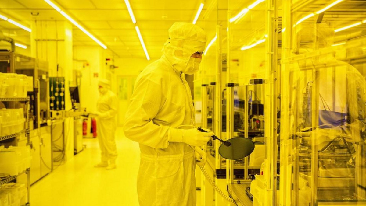
The Fraunhofer Institute for Organic Electronics, Electron Beam and Plasma Technology FEP is one out of 76 institutes and research units of the Fraunhofer-Gesellschaft e. V., the largest European institution for applied research. The core competences of Fraunhofer FEP are electron beam technologies, vacuum thin film deposition techniques and technologies for organic electronics, microdisplay technology and sensors. Main activities target development and adaption of the thin film deposition technologies to a wide range of industrial applications. Fraunhofer FEP runs multiple pilot-scale vacuum coating systems.
Furthermore, Fraunhofer FEP has a unique position in designing microelectronic integrated circuits and components with application- and customer-specific adaptations of silicon circuit foundries’ CMOS processes, that allow their CMOS backplane wafers to be subsequently processed with O/LED frontplane coatings, for example. This subsequent processing is used in particular for extending silicon CMOS wafer functionality with optical and photonic components, such as for high-resolution O/LED microdisplays.
It has to be mentioned that the Fraunhofer activities in Microdisplays & Sensors had started more than 15 years ago and focused around OLED-on-Silicon integration originally. Now Fraunhofer FEP has a very unique offer in providing the full microdisplay device value chain of both CMOS backplane design and OLED frontplane integration as a single source, i.e., device designers and process technology engineers working together continuously, including their strong links to commercial CMOS backplane suppliers (silicon foundries), accessing advanced CMOS process nodes with specifically adapted backends to achieve compatibility for OLED frontplane integration. This long-time experience has been a unique basis for extending our work in backplane capabilities towards µLED frontplane integration as well. Therefore, we assume to be able to substantially contribute to the MIA scope.
Can you say why you joined the microLED association and what it is you hope to achieve?
For many years we have been in good contact and cooperation with Metalgrass, OLED-info and now also MicroLED Association. Due to the rapid developments in the display industry in general as well as microdisplays in particular, it is important to have networks and associations like MIA, that bundle these activities and discuss and inform about the latest trends.
We very much appreciate to be part of this network and get in touch with other members of the MicroLED Association for collaboration and networking. In addition, we would also like to use this excellent network as a basis for communicating and publishing our latest research results regarding our O/LED-microdisplay and sensor developments. As an application-oriented research institute, networking and discussing latest trends, requirements and technologies with possible partners, manufacturers or customers from all around the world is of high importance for us in order to research and develop customer-specific and suitable microdisplay components and sensors based on O/LED-on-silicon technology. Therefore, we look forward to many interesting events and opportunities of MicroLED Association to connect with other members and be an active part of the network.
What is your biggest challenge, and success to date in the microLED industry?
Since the first beginnings with very small devices, which had a limited lifetime and moderate resolutions, very much progress has been made. Fraunhofer FEP now offers a wide range of R&D for customized O/LED microdisplays and sensors as well as evaluation kits for them. An outstanding achievement has been the invention of bi-directional microdisplays, which combine display pixels (image display) and photodetector pixels (image sensor) intersected to each other on a single chip. This had been followed by great results to design ultra-low power OLED microdisplays. These developments even led to a very successful transfer to industry. Together with Microoled (France), we have even been awarded the Franco-German Business Award for this in 2017. In the same year, we were pleased to also host SID-ME and welcome over 100 attendees and high-level international speakers from the field of microdisplays in Dresden, Germany.
The unique backplane design for ultra-low power O/LED microdisplays has led to a number of further developments such as multi-color or ultra-bright devices. Furthermore, we are now able to offer these ultra-low power display developments in certain sample quantities for enabling early customer and application-specific evaluations and validations in system environments.
Besides this, a wide range of full-color micro-displays for AR and VR applications has also been realized within various publicly funded projects, typically in collaboration with industry partners and according to their respective requirements.
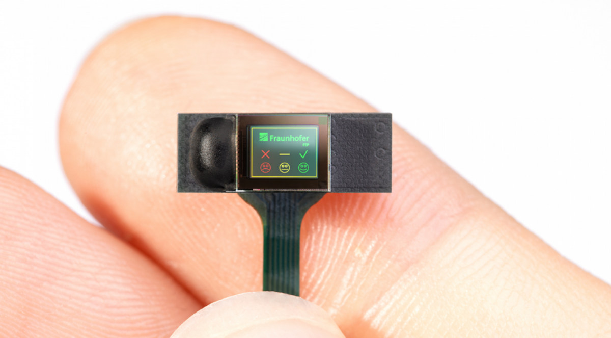
Our most recent success has been the development of an OLED microdisplay with 10,000 dpi developed in 28nm technology. This has been world record and an as-yet unattained level in the global OLED microdisplay market (as of 8/2023). Its backplane has been designed explicitly to be compatible to µLED (and LCOS) frontplanes as well.
As an application-oriented research and development institute, we are facing many unsolved topics and it is our goal to develop suitable solutions and processes that help our partners in industry to be able to realize their innovative ideas. Some of our next topics, that we want to address, are e.g. the development of processes for semi-transparent microdisplays, or the use of new technologies such as quantum dots.
Can you detail your latest prototype/demonstration?
In 2023 Fraunhofer FEP achieved to realize OLED microdisplays for the first time in a 28-nanometer backplane technology on 300mm wafers within the project “Backplane”, funded by the Saxon State Ministry of Economics, Labor and Transport. Components with a display diagonal of 0.18 inches and pixel sizes of only 2.5 micrometers have been manufactured. This corresponds to a pixel density of 10,000 dpi. These unique OLED microdisplays have been presented for the first time at SID Display Week in Los Angeles in May 2023.
How do you see microLEDs changing the display industry in the next 5-10 years?
A major effect of moving towards µLED displays (either flat-panel displays or microdisplays) is the convergence of display technology with semiconductor technology. µLED chips are being manufactured by microelectronics process technology on wafer-level, though wafer substrate and semiconductor materials, sizes and some process steps (incl. tool equipment) differ from each other. Through µLED emitters in flat-panel displays there is now good chance for semiconductor companies to extend their markets into display products well beyond driver chips, and for microdisplays it is an even closer convergence of the semiconductor backplane experience to the µLED frontplane integration approaches. In conclusion, µLED displays will benefit from advances in microelectronics in general, and recent world-wide public and private investments in sustainable and resilient semiconductor supply chains.
µLED might also support emergence of advanced display features, e.g., ultra-compact head-up displays and micro-projectors, transparent displays and new form factors, e.g., curved displays, for enabling innovative performance features and system integration solutions. As an example, by combining a microdisplay chip together with a microprocessor chip (with embedded AI), external connectivity and imaging optics in a single module (chiplet) can enable completely new levels of complexity at very small form-factor, increased reliability and lower cost.
Thank you Dr. Vogel, good luck to you and the Fraunhofer FEP!