We're happy to interview Comptek Solutions, as part of our new series of interviews with MicroLED Industry Association members. Comptek, established in 2017 as a spin-off from the university of Turku, Finland, develops quantum technology (branded as Kontrox) that boosts the performance of devices such as microLEDs and lasers.
Q: Hello! Can you introduce your company and technology?
Vicente Calvo, Comptek's CEO and co-founder: Comptek Solutions is a forerunner in III-V compound semiconductor surface engineering. We have developed a novel surface treatment process - Kontrox - which effectively passivates the surface of the materials by forming a high-quality native crystalline oxide layer with very low surface defect state density. In µLEDs, Kontrox is applied to the chip sidewalls to prevent non-radiative recombination mechanisms, effectively passivating the surface. This drastically improves the performance and manufacturing yields of µLEDs, particularly at small chip sizes.
Q: Can you say why you joined the microLED association and what you hope to achieve?
The association is a perfect networking platform offering an excellent outlook on the current developments and trends in the µLED industry. We particularly appreciate the opportunity to connect to key industry players.
What is your biggest challenge and success to date in the microLED industry?
With every new customer project, our biggest challenge remains the same: the initial development of customized cleaning and passivation process recipes for each chip type. Since the architecture, quality, and composition of the stack differ from customer to customer, this initial work requires considerable effort from the R&D team; but the reward is as significant - once we succeed and obtain optimal results, chip efficiency is improved tremendously. For some customers, we have achieved up to 250% wall plug efficiency improvement compared to conventional passivation with ALD coatings.
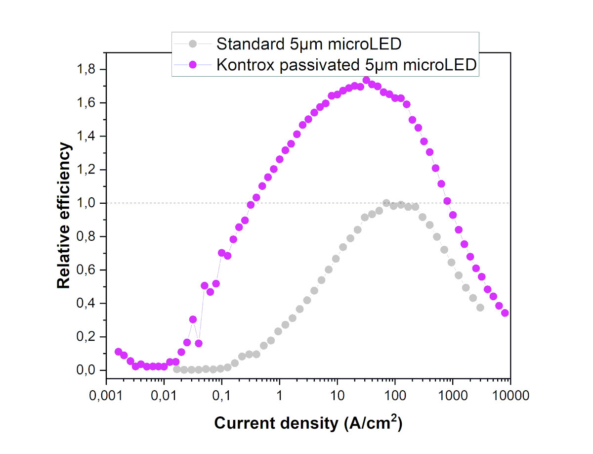
Figure 1:EQE vs Current density in a 5µm GaN µLED
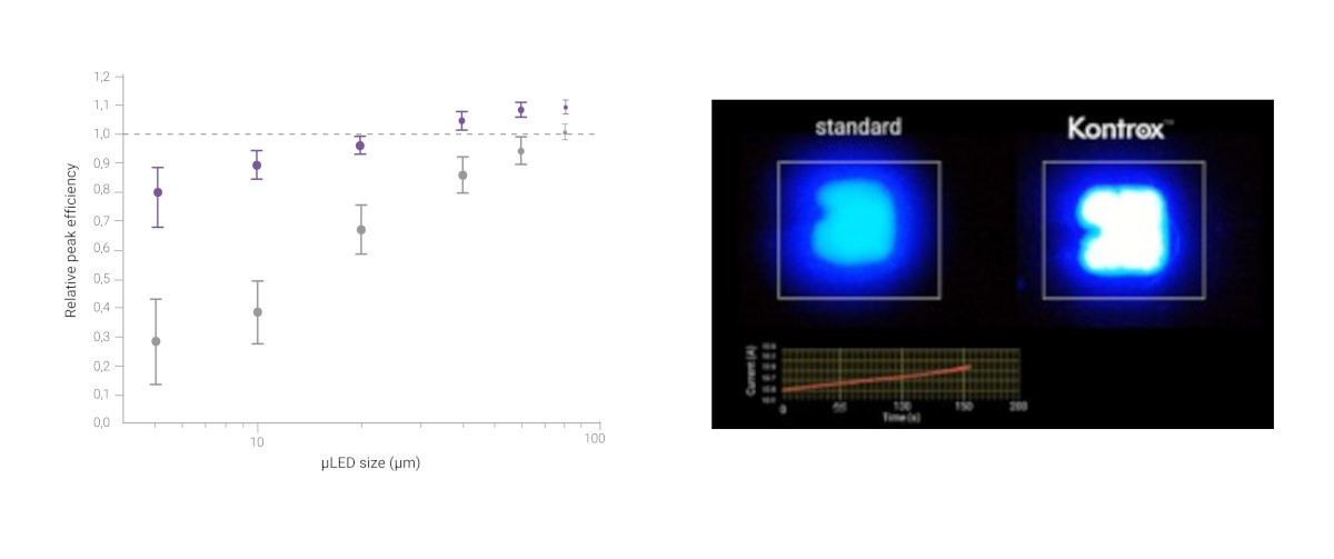
Figure 2:Effect of Kontrox passivation in EQE for different GaN based µLED chip sizes and real EL measurements for 10µm µLEDs
Q: Can you detail your latest prototype/demonstration?
We have recently built the 1st passivation tool prototype optimized for edge emitting lasers; now we are piloting it in collaboration with 2 customers. The machine can also be used to passivate small substrates (2”) of very special material sets for e.g., photonic quantum applications where we also have a first customer. Recently we have been awarded with funding from the European Innovation Council to We are also building build a pilot line to apply Kontrox to 8” substrates in combination with other techniques such as ALD - the tool will be utilized for several significant customer projects in µLED and power electronic applications.

Figure 3:Laser facet Kontrox passivation tool
Q: How do you see microLEDs changing the display industry in the next 5-10 years?
There are still many challenges to be solved at different stages of the manufacturing process. Still, the commercial introduction is getting closer for applications where volumes and tech requirements are not so high, I'd say we'll get there in 1-3 years.
For large displays, driving cost down is the critical challenge, which has to do with low manufacturing yields. But as chip sizes, in this case, are not necessarily the smallest ones, I believe some technological developments, like Kontrox, could help improve the situation in the short-to-mid term. On the other hand, dealing with sizes close to 1µm for very high-resolution displays (such as AR/VR applications) is still very difficult due to extremely low yields and poor chip uniformity within a wafer and from wafer to wafer. Therefore, coming up with efficient solutions and reaching the technology maturity for mass production in this segment might take well over 7-10 years.