Researchers at MIT have developed a bottom-up approach for precise and scalable formation of perovskite nanocrystal arrays with deterministic control over size, number, and position. This new technology enables the deposition of halide perovskite nanocrystals with precise control over the location and size of each individual crystal, integrating them into nanoscale light-emitting diodes.
The researchers demonstrated deterministic arrays of CsPbBr3 nanocrystals with tunable dimensions down to <50 nm and positional accuracy <50 nm.
Halide perovskite materials have largely been implemented into thin-film or micron-sized device applications. Precisely integrating these materials at the nanoscale could open up even more remarkable applications, like on-chip light sources, photodetectors, and memristors. One possible application is also the creation of microLEDs, directly on substrates at large scale - which could have dramatic implications for microLED displays - this technology could be used to create the LEDs on the display backplane, a monolithic approach that does not require a transfer process
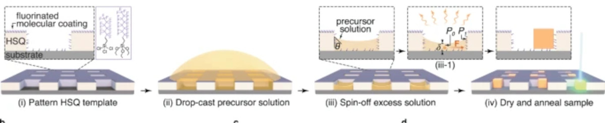
Achieving the integration of perovskite materials at nanoscale has remained challenging because this delicate material can be damaged by conventional fabrication and patterning techniques.
To overcome this obstacle, the MIT team created a technique that allows individual halide perovskite nanocrystals to be grown on-site where needed with precise control over location, to within less than 50 nanometers. (A sheet of paper is 100,000 nanometers thick.) The size of the nanocrystals can also be precisely controlled through this technique, which is important because size affects their characteristics. Since the material is grown locally with the desired features, conventional lithographic patterning steps that could introduce damage are not needed.
