US-based parallel microLED assembly technology developer VerLASE Technologies reports today that it has achieved substantial progress in its mass transfer process for micro-LED displays.
VerLASE now plans to develop the process flow for an assortment of dies sizes from 200 X 200 um (mini-LEDs) down to 10 X 10 um and eventually also 5x5 um. VerLASE plans to demonstrate the transfer of both flip-chip, and vertical thin film LED architectures.
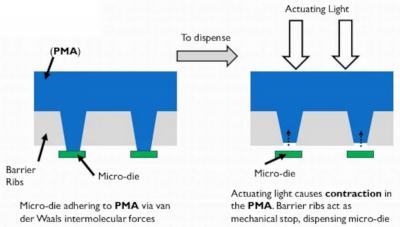
VerLASE's technology is based on a unique technology which it calls Photo-Mechanical Actuation (PMA). This is based on a transfer stamp architecture along with novel chemistry that can deterministically pick-up a large number of microdies, translate them to the desired drop-off location on a substrate and then dispense them with very high accuracy and speed. The company asserts its process once fully implemented is capable of very high transfer throughput rates with high spatial accuracy.


