KAIST

The Korea Advanced Institute of Science and Technology (KAIST), a national research university located in Daejeon, South Korea, has many microLED research activities.

KAIST researchers develop a universal selective transfer process via micro-vacuum force

Researchers from Korea's KAIST institute developed a new microLED selective mass transfer process based on micro-vacuum force. The researchers brand their technology as micro-vacuum assisted selective transfer printing (µVAST), and say that it can be used to transfer a large number of microLEDs by adjusting the micro-vacuum suction force.

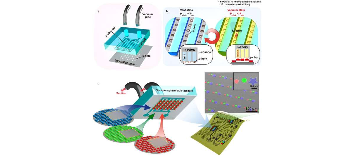
The process starts by forming small (20 micron, in the researchers demonstration device) holes on glass substrates using fast (7000 holes-per second) laser-induced etching (LIE). The LIE-drilled glass substrate is then connected to vacuum channels, which are controlled for selectively picking up, and the releasing, microLED devices.

Read the full story Posted: Dec 21,2023

KAIST researchers discover a way to create microLEDs that are not sensitive to sidewall defects

Researchers from Korea's KAIST have found that by changing the epitaxial structure of microLEDs, it is possible to fundamentally resolve the problem of efficiency degradation in microLED devices. In other words, it is possible to create microLEDs in which the efficiency does not drop with size. 

The researchers discovered that the specific epitaxial structure of the microLED changes how the current drives to the sidewall of the microLEDs. Based on that, the researchers developed a epitaxial structure that is not sensitive to sidewall defects. The proposed structure also reduces generated heat by about 40% compared to standard microLEDs.

Read the full story Posted: Mar 27,2023

KAIST researchers use an array of microLEDs to create a wearable skin care patch

Researchers from Korea-based KAIST institute developed a microLED-powered wearable patch that acts as an UV-induced inhibitor for melanogenesis, the creation of brown or dark pigments that can lead to skin diseases.

LEDs have been used to photo-stimulate in skin care, but normal devices cannot conform to the skin shape, they operate from a distance which is problematic. If the patch is connected to the skin, it achieves much more effective photo-treatment. In this research, the team fabricated a 4x4 cm2 wearable device made from an array of 100-micron sized microLED chips, vertically interconnected for high flexibility.

Read the full story Posted: Nov 23,2022

KAIST researchers use 3D stacked MicroLEDs to enable high density displays

Researchers from the Korea Advanced Institute of Science and Technology (KAIST) developed a new process that enables the fabrication of highly dense MicroLED displays - up to 63,500 PPI (!).

The technique involves stacking RGB LEDs in three dimensions and a semiconductor patterning process. Stacking LEDs one on top of the other creates color interference issues, and to overcome this the researchers deposited an insulating film between the layers. This also improved the efficiency of the microLED devices.

Read the full story Posted: Jan 08,2020

KAIST researchers develop flexible vertical micro-LEDs using an ACF-based transfer process

Researchers from Korea's KAIST developed flexible vertical micro-LEDs (f-VLEDs) using anisotropic conductive film (ACF)-based transfer and interconnection technology.

The researchers developed their own transfer equipment and used it to fabricate a 50x50 array of f-VLEDs using simultaneous transfer and interconnection through the precise alignment of ACF bonding process. The researchers report that the micro-LEDs achieved an optical power density of 30 mW/mm2 - which is three times higher than that of lateral micro LEDs. The LEDs offer improving thermal reliability and lifetime by reducing heat generation within the thin film LEDs.

Read the full story Posted: Feb 18,2018