Avicena, a developer of microLED-based chip-to-chip interconnects, is showing the world's first 1Tbps microLED-based Transceiver IC in 16nm finFET CMOS. The company says that its microLED-based LightBundle interconnects offers much lower power and latency, higher bandwidth and lower cost compared to current solutions based on VCSELs or Silicon Photonics.
Avicena's LightBundle interconnect architecture is based on arrays of innovative GaN microLEDs that are integrated directly onto high performance CMOS ICs. Each microLED array is connected via a multi-core fiber cable to a matching array of CMOS-compatible PDs.
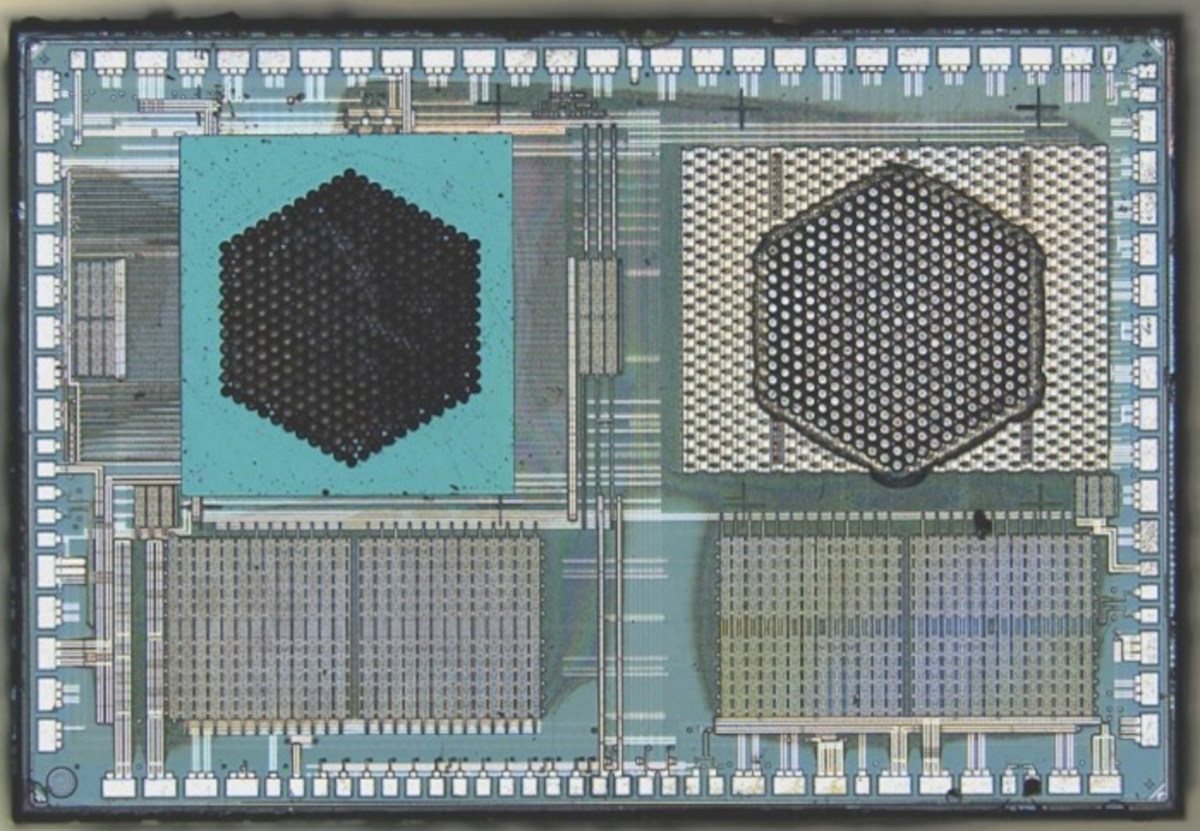
The new 16 nm finFET process ASIC offers an aggregate bandwidth of over 1Tbps bi-directional at 4Gbps per lane. The complete ASIC measures less than 12 mm2 and contains the circuitry for the optical Tx and Rx arrays, as well as a high-speed parallel electrical interface and various DFT/DFM functions like BERT, loopbacks, and Open Eye Monitoring (OEM).
In April 2022, Avicena raised $25 million from Samsung Catalyst Fund, Micron Ventures, and others. Later in 2022 the company acquired Nanosys' GaN microLED fab and engineering team. Avicena uses the fab and team to develop and produce high-speed GaN microLEDs optimized for its application.
The GaN microLED fab was previously owned by glō (before it was acquired by Nanosys), which invested over $200 million in the facilities, which include epitaxy, wafer processing, and lift-off and transfer tools to post-process silicon ICs with optical interfaces.

