How will Apple's withdrawal impact the MicroLED industry?
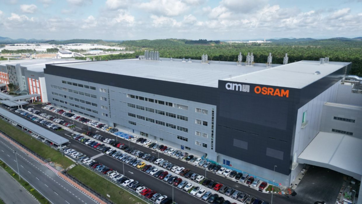
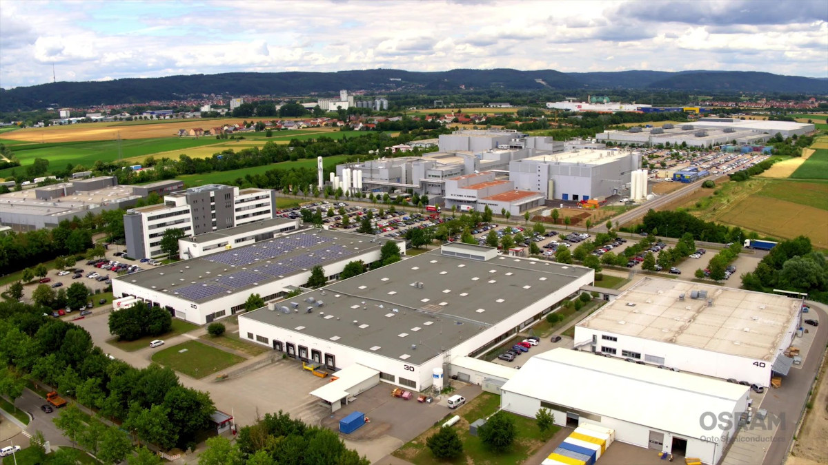
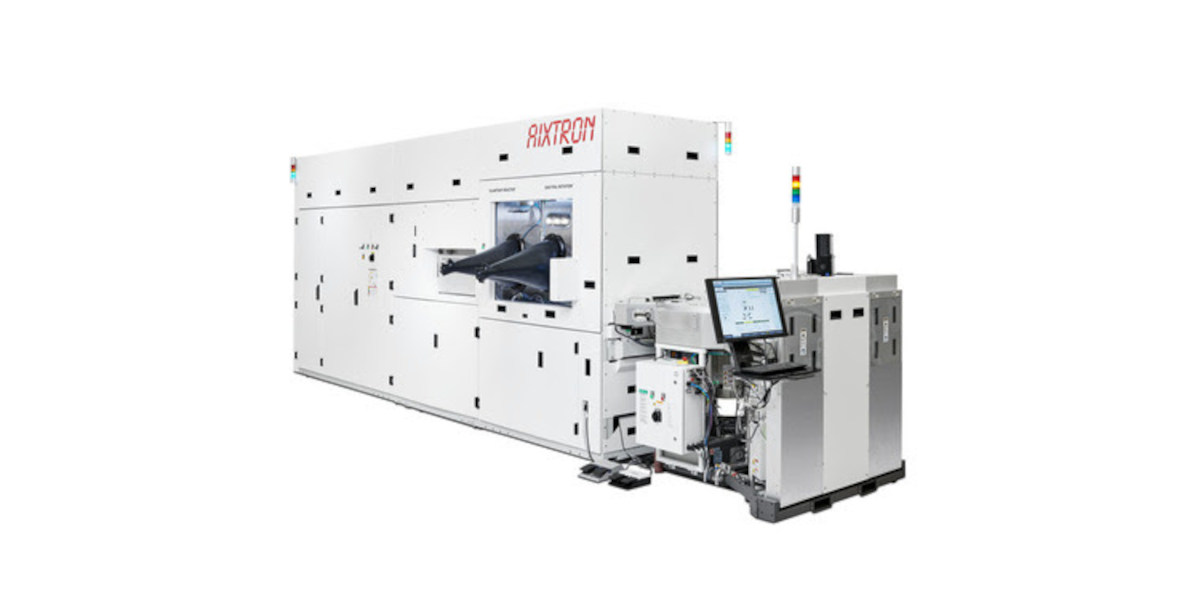
A few days ago, Apple decided to cancel its microLED project with ams-Osram, a development that took the display industry by surprise. It certainly surprised ams-Osram, which announced it will have to re-assess its microLED strategy and incur $650-900 million in impairment charges. It is currently unclear whether Apple's decision was to completely abandon microLED technologies, or if it still in the microLED race, perhaps with different technologies and suppliers. It is likely that Apple does not have any immediate plans to introduce microLED displays, though. In this article, we'll try to analyze the reasons which led to Apple's decision and the probable implications for the microLED industry.
Summary:
- Apple cancels its microLED project with ams-Osram
- We estimate that the main reasons are Apple's technology choice and strategy
- MicroLED production will require next-gen technologies to succeed
- MicroLEDs still pose the best route for the future display technology, but companies will need to realign their strategies
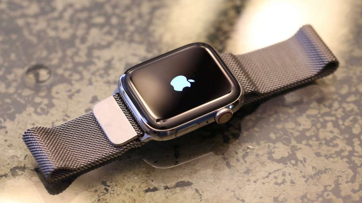
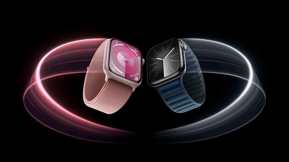
Apple worked on microLED R&D since 2014, with a first target of producing microLED smart watch displays to replace the currently-used AMOLED displays. The Company had several partners, and decided to handle some of the process in-house. It seems as if even after almost 10 years of development and intensive R&D (estimates of Apple's total investment in microLED technology so far range between $1-3 billion USD), the technology was not ready for mass production - at least not at a price that Apple can accept.