XDC installs the world's first 300mm elastomer stamp based microLED transfer tool

MicroLED display technology developer X Display Company (XDC) announced that it installed the world's first 300 mm elastomer stamp based mass MicroLED transfer equipment late in 2020. This tool was installed in the US and the company hopes to start shipping several similar tools for its customers later in 2021.
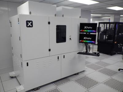
X-Display Corp 300 mm microLED transfer equipment photo

XDC spun out of X-celeprint in 2019 and retained the equipment organization from that transaction. XDC has over 15 years of experience with mass transfer micro printing technologies, and is offering a range of tools for microLED transfer, suitable for R&D work and industrial-scale production.


Read the full story Posted: Feb 04,2021

STRATACACHE to build the first MicroLED production line in the US, mass production expected by 2023

Global digital signage solution provider STRATACACHE is embarking on a project to construct a microLED display production line in Eugene, Oregon. The company aims to start production in this fab at around 2022-2023, with plans to adopt these microLED displays in its own solutions.

The new factory (E4) will be a complete microLED production line, from epiwafer (on 300 mm silicon wafers), through transfer process and to final module assembly. The company plans to produce a wide range of displays, from tablet-sized panels to large-area displays. Some of these displays will be flexible and transparent as the company sees a market demand for such technologies. The yearly capacity of the E4 is expected to start at a 1 million square meters per year.

Read the full story Posted: Jan 25,2021

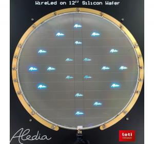
Aledia produces its first nanowire microLEDs on 300 mm silicon wafers

France-based 3D GaN LED developer Aledia announced that it has produced its first nanowire microLED chips on 300 mm silicon wafers, at the CEA-Leti pilot line. Producing microLEDs on large wafers is more cost effective and will enable integration with smaller-node electronics.

Aledia microLED produced on 300mm silicon at CEA-Leti

Earlier this year Aledia announced that it plans to establish a 140 million euros LED production fab in Champagnier, near Grenoble in France. The company already raised 80 million Euros towards that goal. The new fab will use Veeco's 300 mm MOCVD systems.

Read the full story Posted: Dec 16,2020

ALLOS Semiconductor sells its HPE and RF business, to focus on the microLED market

German-based GaN-on-Si developer ALLOS announced that it has sold its high-power electronics and RF business to AZUR SPACE. ALLOS will now focus its business on the microLED display market.

ALLOS Semiconductors developed its GaN-on-Si epiwafer technology for both high power electronics and Micro LED applications, but the time has come to focus on one market. The company says its 200 and 300 mm epiwafer technology is crucial in meeting the uniformity, crystal quality and manufacturability requirements of the novel Micro LED display applications.

Read the full story Posted: Jul 10,2020

ALLOS and Veeco up-scale GaN-on-Si microLED production technology to 300 mm wafers

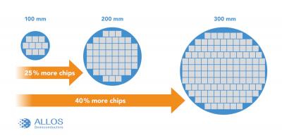
German-based GaN-on-Si developer ALLOS has applied its technology to large 300 mm epiwafers. ALLOS says that scaling up to 300 mm wafers enables higher production efficiencies and thus lower costs. ALLOS estimates that the higher area utilization alone accounts for a cost advantage of 40% compared to standard LED wafers. Standard 300 mm silicon line tools also offer higher production uniformity and yield.

Scaling up from 100 mm to 300 mm silicon wafers (ALLOS Semi)

ALLOS demonstrated the 300 mm scale-up using a reactor made by Veeco who announced selling the first 300 mm GaN reactor to a leading-edge semiconductor fab just some month ago and also showed 300 mm wafer data at CES. ALLOS reports a wavelength uniformity of consistently below 1 nm and "all other production requirements like bow of

Read the full story Posted: Apr 07,2020

MICLEDI explains its MicroLED microdisplay technology and business model

Earlier in January, Belgium-based MICLEDI announced that it raised 4.5 million Euro to develop next-generation MicroLED microdisplays for AR applications.

MICLEDI's team at imec

We had a short talk with MICLEDI's CEO, Sean Lord, who helped us understand a bit more about the company's technology and goals. MICLEDI is indeed focused entirely on the AR market, and so aims to provide display engines that will be extremely bright (over 10 million nits), efficient, and with a very small footprint. In addition costs are also important for the future consumer AR market.

Read the full story Posted: Feb 02,2020

Plessey develops the world's first InGaN on Silicon red LED

UK-based GaN-On-Si MicroLED microdisplay developer Plessey Semiconductor announced that it has successfully developed the world’s first GaN on Silicon-based Red LED.

Plessey native red InGaN LED, on silicon photos

Red LEDs are typically based on AlInGaP materia, or are color-converted from blue LEDs. These red LEDs limit the efficiency and the ability to create ultra-fine pitch sub pixels. Plessey says that InGaN red LEDs will also offer lower manufacturing costs, scalability to larger 200 mm or 300 mm wafers and better hot/cold factor over incumbent AlInGaP-based Red.

Read the full story Posted: Dec 06,2019

Aledia raised $36 million from Intel Capital and existing investors

Aledia logoFrance-based 3D GaN LED developer Aledia announced its Series-C Financing round, totaling $36 million. Its existing investors participated in this round, and Aledia also announced that Intel Capital has joined as a new investor.

Aledia also says that it is developing next-generation Micro-LED displays with several large industrial partners. Aledia is developing both mobile displays (for smartphones, tablets, etc) and micro displays for AR/VR applications.

Read the full story Posted: Feb 07,2018