April 2020

AUO and PlayNitride co-developed a 9.4" 228 PPI flexible automotive-grade microLED display

AU Optronics and PlayNitride announced that the two companies have developed a 9.4" 228 PPI flexible microLED display. The new display is driven by an LTPS backplane and the two companies say it delivers a large color gamut, is weather resistance and it is suitable for automotive applications.
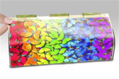
AUO and PlayNitride 9.4-inch 228 PPI flexible micro LED display prototype photo

AUO and PlayNitride has been collaborating on microLED display technologies for many years. In early 2019, AUO announce it plans to accelerate its development of Micro-LED products. The company previous prototype was a 12.1" 1920x720 (169 PPI) panel. In September 2019 AUO's president said that he expects Micro-LED displays to enter the market within 1-2 years, starting with large-area signage and small-sized VR displays.

Read the full story Posted: Apr 23,2020

Yole Developpement: the rate of MicroLED patent filing is rising exponentially

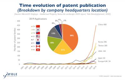
Yole Developpement reports that about 5,500 microLED patents (2,500 patent families) have been filed, by more than 350 organizations. The rate of patent filing is growing exponentially - 40% of the patents were filed in 2019.

Patent publication timeline (2001-2019, Yole Developpement)

According to Yole, the recent patent filing shows that the industry is moving from prototypes to commercial consumer displays. Other notable new finding include that startup companies are a major innovation force, Apple is slowing down with its IP (but this could mean that the company is now focused on commercialization), and Samsung pursues multiple development tracks. BOE is another strong microLED IP player, with almost 150 patent familiies filed in 2019.

Read the full story Posted: Apr 17,2020

ALLOS and Veeco up-scale GaN-on-Si microLED production technology to 300 mm wafers

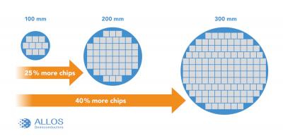
German-based GaN-on-Si developer ALLOS has applied its technology to large 300 mm epiwafers. ALLOS says that scaling up to 300 mm wafers enables higher production efficiencies and thus lower costs. ALLOS estimates that the higher area utilization alone accounts for a cost advantage of 40% compared to standard LED wafers. Standard 300 mm silicon line tools also offer higher production uniformity and yield.

Scaling up from 100 mm to 300 mm silicon wafers (ALLOS Semi)

ALLOS demonstrated the 300 mm scale-up using a reactor made by Veeco who announced selling the first 300 mm GaN reactor to a leading-edge semiconductor fab just some month ago and also showed 300 mm wafer data at CES. ALLOS reports a wavelength uniformity of consistently below 1 nm and "all other production requirements like bow of

Read the full story Posted: Apr 07,2020

Printed Electrochromics boldly goes where no display has gone before


This is a sponsored post by Ynvisible

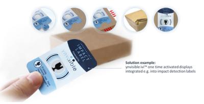
Example use-case for printed electrochromics, Ynvisible
Fig.1 Example use case for printed electrochromics: a shock detector smart label with an interactive printed interface.

Expanding Need for Simple Electronic Display Functionality

Rapid advances in the miniaturization and reduction of costs in computing, electronic sensing, and communications have allowed the integration of “smart” electronic functionality into almost everything. ”Intelligence” is now embedded into a wide range of everyday objects, and spread throughout our working and living environments. Much of this intelligence, data collection and transfer is hidden from the human senses, requiring little or no human involvement. But as the number of human daily touch points and interactions with smart devices grows, so too does the importance of user experience design and the role of displays.

Read the full story Posted: Apr 01,2020

InZiv Ships MicroLED Characterization Equipment

Israel-based display characterization and inspection equipment maker InZiv has recently announced the shipment of a high-resolution pixel characterization tool to an undisclosed Tier-1 consumer electronics company.

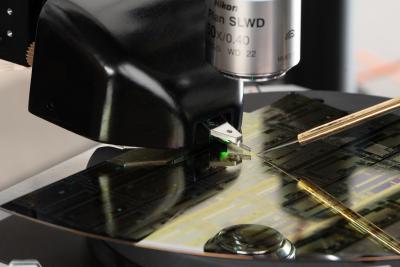
InZiv high-resolution microLED pixel characterization tool closeup photo

InZiv’s tool offers MicroLED defect detection on the wafer and pixel level with unprecedented sub-micron resolutions. Measuring luminescence, spectral wavelengths and 3D structure at the highest resolutions, the equipment enables the identification and the source of defects, accelerating product time to market.


Read the full story Posted: Apr 01,2020